9-11 December 2025
Muscat, Oman
17:00 – 17:45
Panel Session: Breakthrough Innovations, Industry Collaborations and Roadmap
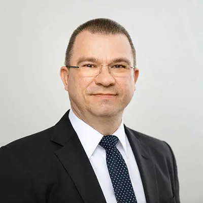
Moderator
Jörg Amelung
Fraunhofer Institute for Photonic Microsystems
Jörg Amelung is Deputy Director of the Fraunhofer Institute for Photonic Microsystems (IPMS) and heads the MEMS Engineering, Manufacturing & Test division. Fraunhofer IPMS is a leading research institute in the MEMS field, equipped with high quality microsystem cleanrooms (200 – 300 mm wafer). As an expert and manager in MEMS technology, Jörg Amelung has been driving the development of smart microsystem technologies since 1993. He also played a key role in OLED development and founded two companies specializing in this field.
Fraunhofer Institute for Photonic Microsystems
Company Profile
Fraunhofer IPMS is a leading international research and development service provider for electronic and photonic microsystems in the application fields of Smart Industrial Solutions, Bio and Health, Mobility as well as Green and Sustainable Microelectronics. Research focuses on customer-specific miniaturized sensors and actuators, MEMS systems, microdisplays and integrated circuits as well as wireless and wired data communication, neuromorphic and quantum computing. Services range from consulting and design to process development and pilot series production.
The Fraunhofer IPMS is one of 75 institutes of the Fraunhofer-Gesellschaft, the leading organization for applied research in Europe. With nearly 32,000 employees Fraunhofer operates with an annual budget of €3.6 billion, €3.1 billion of which is generated by contract research — Fraunhofer’s core business model.
Company Products & Services
The range of services includes wafer processing, characterization & testing, assembly and interconnection technology and the organization of external and supplier services. At the Center Nanoelectronic Technologies (CNT), Fraunhofer IPMS offers applied research, process and material development on 300 mm wafers for microchip producers, suppliers, device manufacturers and R&D partners. 4000 m² of clean room space is available for processing customer orders as well as laboratory space for over 80 processing and analytical tools.

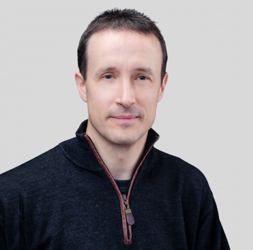
Panelist
Ken Diest
Meta
Ken Diest is a Research Manager and Tech Lead at Meta’s Reality Labs, where he leads programs focused on MEMS and micro-actuator technologies. His focus is on developing these technologies from early stage through production to address critical opto-mechanical and display challenges in AR/MR.
A Materials Scientist by training, Ken’s prior work focused on tunable devices and materials with an emphasis on optical systems. He was the editor and co-author of the book Numerical Methods for Metamaterial Design, and has previously held technology development roles at Apple, MIT Lincoln Laboratories, and Northrop Grumman that focused on new displays and nano-photonics.
Meta
Company Profile
Meta builds technologies that help people connect, find communities, and grow businesses. When Facebook launched in 2004, it changed the way people connect. Apps like Messenger, Instagram and WhatsApp further empowered billions around the world. Now, Meta is moving beyond 2D screens toward immersive experiences like augmented and virtual reality to help build the next evolution in social technology.


Panelist
Alastair Attard
UTAC Group
Alastair Attard is Director of Business Development at UTAC Group. He has a Bachelor’s degree in Mechanical Engineering and an Executive MBA, and brings over 19 years of experience in the semiconductor assembly & test.
Alastair has previously held positions at STMicroelectronics in MEMS and SiP process engineering and package development, and at Besi where he managed the process development group for advanced die attach technologies.
Alastair joined UTAC in 2018 and today is responsible for business development of semiconductor assembly and test solutions with particular focus on MEMS, Sensing, and Advanced Packaging.
UTAC Group
Company Profile
UTAC Group is a leading outsourced semiconductor assembly and test (OSAT) provider, founded in 1997 and headquartered in Singapore. The company specializes in advanced assembly and test services for logic, memory, analog/mixed-signal, image sensors, MEMS, and power devices. UTAC supports a global customer base that includes fabless companies, integrated device manufacturers (IDMs), and wafer foundries.
With ten manufacturing facilities across Singapore, Thailand, China, and Indonesia, and a robust global sales network spanning North America, Europe, Greater China, Japan, and Southeast Asia, UTAC delivers comprehensive turnkey solutions—from wafer probing to final testing.
UTAC serves diverse market segments including automotive, computing, communications, consumer electronics, and industrial applications. Renowned for its reliability, technological expertise, and customer-centric approach, UTAC continues to play a vital role in enabling next-generation semiconductor innovation.
Company Products & Services
UTAC Group provides a comprehensive range of semiconductor assembly and test services, delivering turnkey solutions from wafer probe to final test across key end markets.
Its packaging portfolio includes leadframe-based packages such as QFN, DFN, QFP, TLA, and Cu-clip variants, as well as laminate-based BGA/iBGA packages for mobile, computing, and automotive applications. UTAC also offers System-in-Package (SiP) modules that integrate multiple components into compact, high-density solutions for IoT, wearables, and automotive electronics.
Advanced wafer-level offerings include bumping services and Wafer-Level Chip Scale Packaging (WLCSP) for customers requiring miniaturization, high electrical performance, and low-profile form factors.
UTAC also supports image sensor packaging, including automotive-grade iBGA with cleanroom assembly to meet stringent reliability and contamination standards.
To complement mass production, UTAC provides value-added services such as package design support, reliability qualification, and failure analysis—helping customers accelerate time to market with confidence.

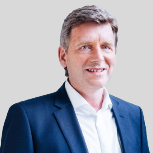
Panelist
Volker Herbig
X-FAB
Volker Herbig, VP BU Microsystems at X-FAB, oversees all MEMS activities within the X-FAB Group. Before assuming his current role, Volker worked as Director Product Marketing at X-FAB. Previously he held also engineering, marketing and management positions at Siemens, Inkjet Technologies and Carl Zeiss where, among other activities, he developed MEMS inkjet print heads and was responsible for setting up a manufacturing facility for those. Volker Herbig holds a master’s degree in physics from Humboldt University, Berlin, Germany.
X-FAB
Company Profile
X-FAB is one of the world’s leading specialty foundry groups for analog/mixed-signal semiconductor technologies with a clear focus on automotive, industrial, and medical applications. As a pure-play foundry, X-FAB provides manufacturing and design support services to customers that design analog/mixed-signal integrated circuits (ICs) and other semiconductor devices for use in their own products or the products of their customers. Its customers worldwide benefit from the highest quality standards, manufacturing excellence and innovative solutions by using X-FAB’s modular CMOS and SOI processes in geometries ranging from 1.0 µm to 110 nm, and its special micro-electro-mechanical systems (MEMS) processes. X-FAB is also the first pure-play foundry to provide comprehensive processing technologies for the wide-bandgap materials silicon carbide (SiC) and gallium nitride (GaN). The GaN-on-Si wafers are manufactured in its modern 8” fab in Dresden, Germany, and SiC wafers in the 6” fab in Lubbock, Texas, USA. X-FAB runs six production facilities in Germany, France, Malaysia and the U.S. The company employs about 4,200 people worldwide.

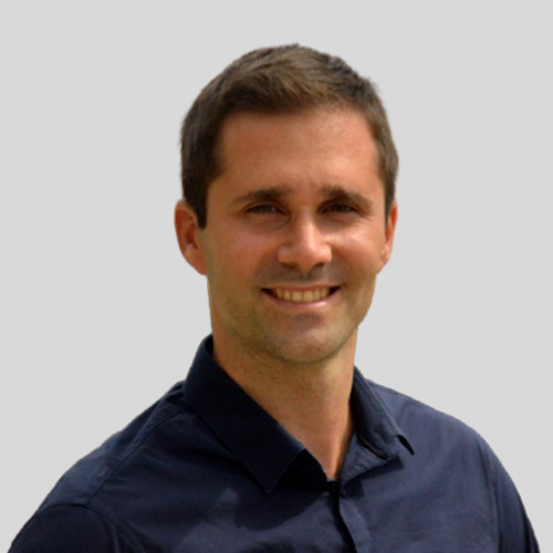
Panelist
Andreja Erbes
STMicroelectronics
Andreja Erbes has been the Director of Technology Scouting and R&D Partnerships at STMicroelectronics since 2022, actively driving innovation initiatives within ST’s Innovation Office. He received the M.Eng., M.A., and Ph.D. degrees from the Department of Engineering, University of Cambridge, in 2011, 2014, and 2015, respectively, specializing in MEMS and mmWave Analog/RF circuit design. He currently serves as Vice President of the IEEE Ultrasonics, Ferroelectrics, and Frequency Control Society (IEEE UFFC).
STMicroelectronics
Company Profile
At ST, we are more than 50,000 creators and makers of semiconductor technologies mastering the semiconductor supply chain with state-of-the-art manufacturing facilities. An integrated device manufacturer, we work with more than 200,000 customers and thousands of partners to design and build products, solutions, and ecosystems that address their challenges and opportunities, and the need to support a more sustainable world. Our technologies enable smarter mobility, more efficient power and energy management, and the wide-scale deployment of cloud-connected autonomous things. We are committed to achieving our goal to become carbon neutral on scope 1 and 2 and partially scope 3 by 2027. Further information can be found at www.st.com.

Panelist
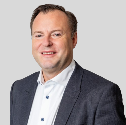
Tomas Bauer
Silex Microsystems
With over 20 years at Silex Microsystems, Tomas Bauer has been a driving force behind the company’s global leadership in MEMS innovation. As Executive Vice President of Sales & Business Development, he has played a central role in shaping Silex’s strategic roadmap and fostering long-term collaborations with leading technology innovators. A mechanical engineer by training, Tomas began his career at Ericsson’s wafer fab, where he bridged engineering and commercial roles. Since joining Silex in 2004, his deep industry insight and commitment to breakthrough partnerships have helped position the company at the forefront of next-generation MEMS manufacturing and ecosystem development.
Silex Microsystems
Company Profile
Silex Microsystems AB, a Swedish company, is the world’s leading pure-play MEMS foundry, trusted by the most innovative companies to bring breakthrough ideas to market—faster.
With unmatched expertise and advanced MEMS manufacturing capabilities, Silex turns groundbreaking designs into manufacturable, scalable products, from concept to high-volume production.
Our cutting-edge wafer fab, combined with industry leading process technologies, empowers customers to scale disruptive solutions with confidence, speed, and quality.
