27-28 August 2025
Suwon
Strategy and role for Data Center, AI and EV?
07:00 – 08:00
Registration & Networking Coffee
07:15 – 08:15
Registration
07:30 – 08:30
Registration
07:30 – 08:50
Registration
07:30 – 08:15
Registration
07:30 – 08:30
Registration
07:30 – 08:30
Registration
07:30 – 08:30
Registration
07:30 – 08:10
Registration
08:00 – 08:40
Registration
08:00 – 08:15
Opening Remarks
Welcome Address by I.S.I.G.
Summit Overview: Key Themes & Objectives
08:00 – 08:35
Registration
08:00 – 08:40
Registration
08:10 – 08:30
ISIG 15th Year Anniversary Welcome

Salah Nasri
International Semiconductor Industry Group (I.S.I.G.)
Salah Nasri leads the International Semiconductor Industry Group, founded in 2010, it is a global leading semiconductor association known for its flagship platforms (The International Semiconductor Executive Summits), uniting top executives, government officials, researchers, and investors from around the globe to address challenges and opportunities in chip manufacturing and technology innovation. He guides the association in shaping crucial industry dialogues—ranging from trade regulations to cutting-edge chip design—and fosters collaborations that drive the future of the semiconductor sector. Salah studied International Relations and Economics at Oxford University, Loughborough University and in 2024 graduated from the Stanford Graduate School of Business Executive Program.
Company Profile
Established in 2010, the International Semiconductor Industry Group (ISIG) is a prestigious and trusted global platform, known for fostering collaboration and driving innovation across the semiconductor industry. With a strong foundation through its International Semiconductor Executive Summits (I.S.E.S.), ISIG orchestrates influential regional summits across the U.S., Middle East, Europe and Asia, fully endorsed by local governments and leading companies throughout the semiconductor supply chain.
At ISIG, we are more than just event organizers—we serve as a catalyst for shaping the future of the semiconductor industry. Through high-level executive recruitment, expert consultation, and strategic investor engagement, ISIG empowers global collaboration, helping industry leaders connect, collaborate, and innovate. Our vision is to create a trusted network that transcends borders and disciplines, uniting government officials, academic experts, and investors to tackle the most pressing challenges and seize the greatest opportunities in the semiconductor ecosystem.
Together, we ensure the semiconductor industry remains at the forefront of technological advancement and economic growth, shaping a sustainable future for the global market.


Saeed Amidi
Plug and Play Tech Center
Saeed is a seasoned investor and executive with over 30 years of experience growing businesses in numerous industries, including real estate, bottled water, packaging, and technology investing. Following the early success of his various businesses, The Amidi Group initially purchased a building in Palo Alto and decided to rent the extra office spaces to startups.
As the CEO and founder of Plug and Play, Saeed applies his passion for the tech industry daily by working with forward-thinking partners and the best global startups to facilitate positive change worldwide. Since Plug and Play’s launch in 2006, the company has worked with over 90,000 startups, made over 2,000 investments, and boasts over 30 unicorns including Dropbox, PayPal, Lending Club, N26, and Honey. Similar to his unexpected success with the “Lucky Building,” Saeed considered himself lucky overall when he moved to Silicon Valley in the late 70s, where he was then unaware of the ecosystem it would become.
Company Profile
Plug and Play is the ultimate innovation platform. Our mission is to build the world’s leading innovation platform and make innovation open to anyone, anywhere. We do this by connecting entrepreneurs, corporations, and investors worldwide.
Over the past 15 years, we have brought together 35,000+ startups, 500+ world-leading corporations, and hundreds of venture capital firms, universities, and government agencies across 20+ industries.
We are active in 50+ locations globally, including the U.S., China, France, Germany, South Africa, Singapore, Indonesia, Brazil, and more.
Together with our partners, we are creating a unique ecosystem designed to facilitate meaningful introductions, invest in startups, and bring together key stakeholders.
The industries we focus on include Agtech, Animal Health, Brand & Retail, Crypto & Digital Assets, Energy, Enterprise, Fintech, Food & Beverage, Health, Insurtech, IoT, Maritime, Media & Ad, Mobility, New Materials & Packaging, Real Estate & Construction, Smart Cities, Supply Chain, Sustainability, and Travel & Hospitality.


Rouzbeh Borhani
Plug and Play Tech Center
Rouzbeh is the Founder and Head of the Semiconductor practice at Plug and Play, the largest corporate innovation platform in the world and one of the most active early-stage investors globally. He collaborates closely with entrepreneurs, corporate innovation leaders, and investors, focusing on the semiconductor industry value chain.
Previously, Rouzbeh served as the Country Retail Management Director in the Consumer Electronics sector.
Rouzbeh holds a Master of Business Administration and a Master of Science in Disruptive Innovation, along with a Bachelor of Science in Mechatronics Engineering. He is currently a PhD candidate in Electrical and Computer Engineering. His passion lies at the intersection of technology and business.
Company Profile
Plug and Play is the ultimate innovation platform. Our mission is to build the world’s leading innovation platform and make innovation open to anyone, anywhere. We do this by connecting entrepreneurs, corporations, and investors worldwide.
Over the past 15 years, we have brought together 35,000+ startups, 500+ world-leading corporations, and hundreds of venture capital firms, universities, and government agencies across 20+ industries.
We are active in 50+ locations globally, including the U.S., China, France, Germany, South Africa, Singapore, Indonesia, Brazil, and more.
Together with our partners, we are creating a unique ecosystem designed to facilitate meaningful introductions, invest in startups, and bring together key stakeholders.
The industries we focus on include Agtech, Animal Health, Brand & Retail, Crypto & Digital Assets, Energy, Enterprise, Fintech, Food & Beverage, Health, Insurtech, IoT, Maritime, Media & Ad, Mobility, New Materials & Packaging, Real Estate & Construction, Smart Cities, Supply Chain, Sustainability, and Travel & Hospitality.


Rouzbeh Borhani
Plug and Play Tech Center
Rouzbeh is the Founder and Head of the Semiconductor practice at Plug and Play, the largest corporate innovation platform in the world and one of the most active early-stage investors globally. He collaborates closely with entrepreneurs, corporate innovation leaders, and investors, focusing on the semiconductor industry value chain.
Previously, Rouzbeh served as the Country Retail Management Director in the Consumer Electronics sector.
Rouzbeh holds a Master of Business Administration and a Master of Science in Disruptive Innovation, along with a Bachelor of Science in Mechatronics Engineering. He is currently a PhD candidate in Electrical and Computer Engineering. His passion lies at the intersection of technology and business.
Company Profile
Plug and Play is the ultimate innovation platform. Our mission is to build the world’s leading innovation platform and make innovation open to anyone, anywhere. We do this by connecting entrepreneurs, corporations, and investors worldwide.
Over the past 15 years, we have brought together 35,000+ startups, 500+ world-leading corporations, and hundreds of venture capital firms, universities, and government agencies across 20+ industries.
We are active in 50+ locations globally, including the U.S., China, France, Germany, South Africa, Singapore, Indonesia, Brazil, and more.
Together with our partners, we are creating a unique ecosystem designed to facilitate meaningful introductions, invest in startups, and bring together key stakeholders.
The industries we focus on include Agtech, Animal Health, Brand & Retail, Crypto & Digital Assets, Energy, Enterprise, Fintech, Food & Beverage, Health, Insurtech, IoT, Maritime, Media & Ad, Mobility, New Materials & Packaging, Real Estate & Construction, Smart Cities, Supply Chain, Sustainability, and Travel & Hospitality.

08:15 – 08:25
Understand the Present; Predict the Future
In this presentation, Mr. Sherman will present examples from the ISIG Chips & Wafers data reports that demonstrate the depth and scope of the information we provide to our customers.
Whether you are a Fabless company, an equipment manufacturer or an OSAT our reports provide the timely data you need to make better decisions.

Simi Sherman
International Semiconductor Industry Group (I.S.I.G.)
Simi Sherman is Co-Founder and CEO of Chips & Wafers, a semiconductor data and research platform, and VP of Research with ISIG.
After six years at a Buy-Side global equities Hedge Fund, where he was a Partner and led semiconductor research, Simi Co-founded Chips & Wafers. Working together with ISIG, Chips & Wafers provides semiconductor companies and investors with timely and actionable data they utilize in making more informed decisions.
Company Profile
Established in 2010, the International Semiconductor Industry Group (ISIG) is a prestigious and trusted global platform, known for fostering collaboration and driving innovation across the semiconductor industry. With a strong foundation through its International Semiconductor Executive Summits (I.S.E.S.), ISIG orchestrates influential regional summits across the U.S., Middle East, Europe and Asia, fully endorsed by local governments and leading companies throughout the semiconductor supply chain.
At ISIG, we are more than just event organizers—we serve as a catalyst for shaping the future of the semiconductor industry. Through high-level executive recruitment, expert consultation, and strategic investor engagement, ISIG empowers global collaboration, helping industry leaders connect, collaborate, and innovate. Our vision is to create a trusted network that transcends borders and disciplines, uniting government officials, academic experts, and investors to tackle the most pressing challenges and seize the greatest opportunities in the semiconductor ecosystem.
Together, we ensure the semiconductor industry remains at the forefront of technological advancement and economic growth, shaping a sustainable future for the global market.

08:15 – 08:30
I.S.I.G. 15th Year Anniversary Opening

Salah Nasri
International Semiconductor Industry Group (I.S.I.G.)
Salah Nasri leads the International Semiconductor Industry Group, founded in 2010, it is a global leading semiconductor association known for its flagship platforms (The International Semiconductor Executive Summits), uniting top executives, government officials, researchers, and investors from around the globe to address challenges and opportunities in chip manufacturing and technology innovation. He guides the association in shaping crucial industry dialogues—ranging from trade regulations to cutting-edge chip design—and fosters collaborations that drive the future of the semiconductor sector. Salah studied International Relations and Economics at Oxford University, Loughborough University and in 2024 graduated from the Stanford Graduate School of Business Executive Program.
Company Profile
Established in 2010, the International Semiconductor Industry Group (ISIG) is a prestigious and trusted global platform, known for fostering collaboration and driving innovation across the semiconductor industry. With a strong foundation through its International Semiconductor Executive Summits (I.S.E.S.), ISIG orchestrates influential regional summits across the U.S., Middle East, Europe and Asia, fully endorsed by local governments and leading companies throughout the semiconductor supply chain.
At ISIG, we are more than just event organizers—we serve as a catalyst for shaping the future of the semiconductor industry. Through high-level executive recruitment, expert consultation, and strategic investor engagement, ISIG empowers global collaboration, helping industry leaders connect, collaborate, and innovate. Our vision is to create a trusted network that transcends borders and disciplines, uniting government officials, academic experts, and investors to tackle the most pressing challenges and seize the greatest opportunities in the semiconductor ecosystem.
Together, we ensure the semiconductor industry remains at the forefront of technological advancement and economic growth, shaping a sustainable future for the global market.

08:20 – 08:50
Keynote: The Future of Fab Operations – Scaling Smart Manufacturing
● Keynote Reserved
08:20 – 08:55
Registration
08:30 – 08:50
Welcome Speech

Salah Nasri
International Semiconductor Industry Group (I.S.I.G.)
Salah Nasri leads the International Semiconductor Industry Group, founded in 2010, it is a global leading semiconductor association known for its flagship platforms (The International Semiconductor Executive Summits), uniting top executives, government officials, researchers, and investors from around the globe to address challenges and opportunities in chip manufacturing and technology innovation. He guides the association in shaping crucial industry dialogues—ranging from trade regulations to cutting-edge chip design—and fosters collaborations that drive the future of the semiconductor sector. Salah studied International Relations and Economics at Oxford University, Loughborough University and in 2024 graduated from the Stanford Graduate School of Business Executive Program.
Company Profile
Established in 2010, the International Semiconductor Industry Group (ISIG) is a prestigious and trusted global platform, known for fostering collaboration and driving innovation across the semiconductor industry. With a strong foundation through its International Semiconductor Executive Summits (I.S.E.S.), ISIG orchestrates influential regional summits across the U.S., Middle East, Europe and Asia, fully endorsed by local governments and leading companies throughout the semiconductor supply chain.
At ISIG, we are more than just event organizers—we serve as a catalyst for shaping the future of the semiconductor industry. Through high-level executive recruitment, expert consultation, and strategic investor engagement, ISIG empowers global collaboration, helping industry leaders connect, collaborate, and innovate. Our vision is to create a trusted network that transcends borders and disciplines, uniting government officials, academic experts, and investors to tackle the most pressing challenges and seize the greatest opportunities in the semiconductor ecosystem.
Together, we ensure the semiconductor industry remains at the forefront of technological advancement and economic growth, shaping a sustainable future for the global market.

08:30 – 08:50
M.S.W.S., I.S.I.G. and P&P Welcome

Salah Nasri
International Semiconductor Industry Group (I.S.I.G.)
Salah Nasri leads the International Semiconductor Industry Group, founded in 2010, it is a global leading semiconductor association known for its flagship platforms (The International Semiconductor Executive Summits), uniting top executives, government officials, researchers, and investors from around the globe to address challenges and opportunities in chip manufacturing and technology innovation. He guides the association in shaping crucial industry dialogues—ranging from trade regulations to cutting-edge chip design—and fosters collaborations that drive the future of the semiconductor sector. Salah studied International Relations and Economics at Oxford University, Loughborough University and in 2024 graduated from the Stanford Graduate School of Business Executive Program.
Company Profile
Established in 2010, the International Semiconductor Industry Group (ISIG) is a prestigious and trusted global platform, known for fostering collaboration and driving innovation across the semiconductor industry. With a strong foundation through its International Semiconductor Executive Summits (I.S.E.S.), ISIG orchestrates influential regional summits across the U.S., Middle East, Europe and Asia, fully endorsed by local governments and leading companies throughout the semiconductor supply chain.
At ISIG, we are more than just event organizers—we serve as a catalyst for shaping the future of the semiconductor industry. Through high-level executive recruitment, expert consultation, and strategic investor engagement, ISIG empowers global collaboration, helping industry leaders connect, collaborate, and innovate. Our vision is to create a trusted network that transcends borders and disciplines, uniting government officials, academic experts, and investors to tackle the most pressing challenges and seize the greatest opportunities in the semiconductor ecosystem.
Together, we ensure the semiconductor industry remains at the forefront of technological advancement and economic growth, shaping a sustainable future for the global market.


Saeed Amidi
Plug and Play Tech Center
Saeed is a seasoned investor and executive with over 30 years of experience growing businesses in numerous industries, including real estate, bottled water, packaging, and technology investing. Following the early success of his various businesses, The Amidi Group initially purchased a building in Palo Alto and decided to rent the extra office spaces to startups.
As the CEO and founder of Plug and Play, Saeed applies his passion for the tech industry daily by working with forward-thinking partners and the best global startups to facilitate positive change worldwide. Since Plug and Play’s launch in 2006, the company has worked with over 90,000 startups, made over 2,000 investments, and boasts over 30 unicorns including Dropbox, PayPal, Lending Club, N26, and Honey. Similar to his unexpected success with the “Lucky Building,” Saeed considered himself lucky overall when he moved to Silicon Valley in the late 70s, where he was then unaware of the ecosystem it would become.
Company Profile
Plug and Play is the ultimate innovation platform. Our mission is to build the world’s leading innovation platform and make innovation open to anyone, anywhere. We do this by connecting entrepreneurs, corporations, and investors worldwide.
Over the past 15 years, we have brought together 35,000+ startups, 500+ world-leading corporations, and hundreds of venture capital firms, universities, and government agencies across 20+ industries.
We are active in 50+ locations globally, including the U.S., China, France, Germany, South Africa, Singapore, Indonesia, Brazil, and more.
Together with our partners, we are creating a unique ecosystem designed to facilitate meaningful introductions, invest in startups, and bring together key stakeholders.
The industries we focus on include Agtech, Animal Health, Brand & Retail, Crypto & Digital Assets, Energy, Enterprise, Fintech, Food & Beverage, Health, Insurtech, IoT, Maritime, Media & Ad, Mobility, New Materials & Packaging, Real Estate & Construction, Smart Cities, Supply Chain, Sustainability, and Travel & Hospitality.


Rouzbeh Borhani
Plug and Play Tech Center
Rouzbeh is the Founder and Head of the Semiconductor practice at Plug and Play, the largest corporate innovation platform in the world and one of the most active early-stage investors globally. He collaborates closely with entrepreneurs, corporate innovation leaders, and investors, focusing on the semiconductor industry value chain.
Previously, Rouzbeh served as the Country Retail Management Director in the Consumer Electronics sector.
Rouzbeh holds a Master of Business Administration and a Master of Science in Disruptive Innovation, along with a Bachelor of Science in Mechatronics Engineering. He is currently a PhD candidate in Electrical and Computer Engineering. His passion lies at the intersection of technology and business.
Company Profile
Plug and Play is the ultimate innovation platform. Our mission is to build the world’s leading innovation platform and make innovation open to anyone, anywhere. We do this by connecting entrepreneurs, corporations, and investors worldwide.
Over the past 15 years, we have brought together 35,000+ startups, 500+ world-leading corporations, and hundreds of venture capital firms, universities, and government agencies across 20+ industries.
We are active in 50+ locations globally, including the U.S., China, France, Germany, South Africa, Singapore, Indonesia, Brazil, and more.
Together with our partners, we are creating a unique ecosystem designed to facilitate meaningful introductions, invest in startups, and bring together key stakeholders.
The industries we focus on include Agtech, Animal Health, Brand & Retail, Crypto & Digital Assets, Energy, Enterprise, Fintech, Food & Beverage, Health, Insurtech, IoT, Maritime, Media & Ad, Mobility, New Materials & Packaging, Real Estate & Construction, Smart Cities, Supply Chain, Sustainability, and Travel & Hospitality.


Rouzbeh Borhani
Plug and Play Tech Center
Rouzbeh is the Founder and Head of the Semiconductor practice at Plug and Play, the largest corporate innovation platform in the world and one of the most active early-stage investors globally. He collaborates closely with entrepreneurs, corporate innovation leaders, and investors, focusing on the semiconductor industry value chain.
Previously, Rouzbeh served as the Country Retail Management Director in the Consumer Electronics sector.
Rouzbeh holds a Master of Business Administration and a Master of Science in Disruptive Innovation, along with a Bachelor of Science in Mechatronics Engineering. He is currently a PhD candidate in Electrical and Computer Engineering. His passion lies at the intersection of technology and business.
Company Profile
Plug and Play is the ultimate innovation platform. Our mission is to build the world’s leading innovation platform and make innovation open to anyone, anywhere. We do this by connecting entrepreneurs, corporations, and investors worldwide.
Over the past 15 years, we have brought together 35,000+ startups, 500+ world-leading corporations, and hundreds of venture capital firms, universities, and government agencies across 20+ industries.
We are active in 50+ locations globally, including the U.S., China, France, Germany, South Africa, Singapore, Indonesia, Brazil, and more.
Together with our partners, we are creating a unique ecosystem designed to facilitate meaningful introductions, invest in startups, and bring together key stakeholders.
The industries we focus on include Agtech, Animal Health, Brand & Retail, Crypto & Digital Assets, Energy, Enterprise, Fintech, Food & Beverage, Health, Insurtech, IoT, Maritime, Media & Ad, Mobility, New Materials & Packaging, Real Estate & Construction, Smart Cities, Supply Chain, Sustainability, and Travel & Hospitality.

08:30 – 08:50
Keynote
AI use cases in semiconductor data analytics and quality management
AI agents are already making waves by improving known applications that long been used by engineers, developers and every day ordinary users. Semiconductor manufacturing alike has been impacted in the areas of data analytics , traceability, commonality study , corner case identification and more. this presentation will go over some of those AI use cases.
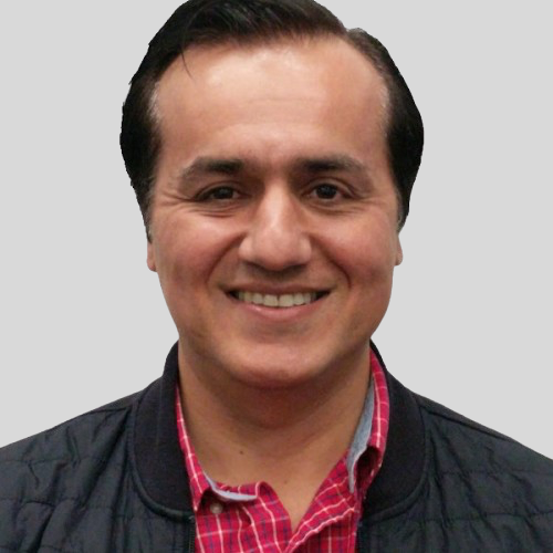
Bizhan Delgoshaei
Bizhan Delgoshaei leads custom silicon engineering operation at google in charge of Tensor manufacturing, test and quality. His career spans over two decades ramping leading edge semiconductor products (FPGA, Memory and Storage, SoC and PMIC, Security Chips and more) from new product introduction to high volume manufacturing. Bizhan has led product engineering , supplier quality engineering and engineering operation organizations in Fabless Semiconductor companies such as Altera, Apple and Google. He holds a masters degree in VLSI from University of Southern California and BS in Electrical Engineering from Sharif University of Technology, Tehran Iran.
Company Profile
A problem isn’t truly solved until it’s solved for all. Googlers build products that help create opportunities for everyone, whether down the street or across the globe. Bring your insight, imagination and a healthy disregard for the impossible. Bring everything that makes you unique. Together, we can build for everyone.

08:30 – 08:45
M.S.W.S. & I.S.I.G. Welcome
08:35 – 08:55
Keynote
Next-Generation GaN/SiC To Accelerate Electrification
New developments in both GaN and SiC combined with new power systems architecture are creating new opportunities to accelerate electrification of our planet across multiple, major markets including electric transportation, renewables, energy storage and more. Technology details, application examples and market implications will be presented.

Gene Sheridan
Navitas Semiconductor
Gene Sheridan brings over 25 years of experience in power management & semiconductors with an impressive track record in creating, leading and scaling businesses that have enjoyed excellent value creation, growth and profitability.
Most recently, Gene served as CEO of the VC-backed semiconductor start-up BridgeCo that captured 80% market share in the wireless audio market before a successful sale to Standard Microsystems Corporation (SMSC). Prior to BridgeCo, Gene served as VP & GM at International Rectifier where he managed a business unit with a team of over 100 employees and $600M annual revenues.
At IRF, Gene held several positions that spanned engineering, manufacturing, sales & marketing including the creation of a $70M/yr start-up. Gene holds a BSEE from Clarkson University.
Company Profile
Founded in 2014, Navitas develops ultra-efficient gallium nitride (GaN) semiconductors that are revolutionizing the world of power electronics in terms of efficiency, performance, size, cost and sustainability.
GaN is growing in importance because of its ability to offer significantly improved performance over conventional silicon semiconductors while reducing the energy and the physical space needed to deliver that performance. GaN technology will accelerate the transition to a sustainable future by delivering efficiency improvements, lowering the cost of clean energy and reducing the materials and energy needed to create power semiconductors.
Navitas is the industry leader in GaN with drive, control and protection in a single easy-to-use integrated circuit (IC). Navitas GaNFast ICs are easy-to-use ‘digital in, power out’ building blocks that enable up to one hundred times faster switching speeds while increasing energy savings by as much as 40%.

08:35 – 08:50
Welcome

Saeed Amidi
Plug and Play Tech Center
Saeed is a seasoned investor and executive with over 30 years of experience growing businesses in numerous industries, including real estate, bottled water, packaging, and technology investing. Following the early success of his various businesses, The Amidi Group initially purchased a building in Palo Alto and decided to rent the extra office spaces to startups.
As the CEO and founder of Plug and Play, Saeed applies his passion for the tech industry daily by working with forward-thinking partners and the best global startups to facilitate positive change worldwide. Since Plug and Play’s launch in 2006, the company has worked with over 90,000 startups, made over 2,000 investments, and boasts over 30 unicorns including Dropbox, PayPal, Lending Club, N26, and Honey. Similar to his unexpected success with the “Lucky Building,” Saeed considered himself lucky overall when he moved to Silicon Valley in the late 70s, where he was then unaware of the ecosystem it would become.
Company Profile
Plug and Play is the ultimate innovation platform. Our mission is to build the world’s leading innovation platform and make innovation open to anyone, anywhere. We do this by connecting entrepreneurs, corporations, and investors worldwide.
Over the past 15 years, we have brought together 35,000+ startups, 500+ world-leading corporations, and hundreds of venture capital firms, universities, and government agencies across 20+ industries.
We are active in 50+ locations globally, including the U.S., China, France, Germany, South Africa, Singapore, Indonesia, Brazil, and more.
Together with our partners, we are creating a unique ecosystem designed to facilitate meaningful introductions, invest in startups, and bring together key stakeholders.
The industries we focus on include Agtech, Animal Health, Brand & Retail, Crypto & Digital Assets, Energy, Enterprise, Fintech, Food & Beverage, Health, Insurtech, IoT, Maritime, Media & Ad, Mobility, New Materials & Packaging, Real Estate & Construction, Smart Cities, Supply Chain, Sustainability, and Travel & Hospitality.

Day 2 Morning Session Moderator

Kuan-Neng Chen, Ph.D.
NYCU
Dr. Kuan-Neng Chen is Dean of International College of Semiconductor Technology and Chair Professor at Institute of Electronics at National Yang Ming Chiao Tung University (NYCU) in Taiwan. He received his Ph.D. degree in Electrical Engineering and Computer Science, as well as his M.S. degree in Materials Science and Engineering, both from Massachusetts Institute of Technology (MIT). Dr. Chen has held several prominent positions including Vice President for International Affairs, Associate Dean of International College of Semiconductor Technology at NYCU, Program Director of the Micro-Electronics Program at National Science and Technology Council in Taiwan, Adjunct R&D Director at Industrial Technology and Research Institute (ITRI), and Research Staff Member at IBM Thomas J. Watson Research Center.
Dr. Chen has received numerous awards and honors throughout his career, including IEEE EPS Exceptional Technical Achievement Award, IMAPS William D. Ashmon – John A. Wagnon Technical Achievement Award, National Industrial Innovation Award, MOST/NSTC Outstanding Research Award (twice), MOST/NSTC Futuristic Breakthrough Technology Award (twice), Pan Wen Yuan Foundation Outstanding Research Award, CIE Outstanding Professor Award, CIEE Outstanding Professor Award, and IBM Invention Achievement Awards (5 times). He has authored over 400 publications, including 3 books and 7 book chapters, and holds 88 patents. Dr. Chen served as Guest Editor for the MRS Bulletin, IEEE Transactions on Components, Packaging, and Manufacturing Technology, and Materials Science in Semiconductor Processing, and has held leadership roles in various conferences and committees, such as IEEE IITC General Chair. Dr. Chen is Fellow of National Academy of Inventors (NAI), IEEE, IET, IMAPS, and CIEE and member of Phi Tau Phi Scholastic Honor Society.
Additionally, Dr. Chen is Specially Appointed Professor at Institute of Tokyo Science (previously Tokyo Tech). His current research interests focus on three-dimensional integrated circuits (3D IC), advanced packaging, and heterogeneous integration.
Company Profile
NYCU was founded on the idea that, in a great university, people work across the disciplines to solve real-world problems. At our university, putting this idea into practice requires integrating Chiao Tung’s strengths in information and communications technology with Yang Ming’s strengths in biomedical research. It also requires contributing to fields located at the intersection of these research areas, for example, digital medicine and bioinformatics. And it requires training our students in such a way that the next generation will not be as constrained by disciplinary boundaries as the previous one.
At NYCU, we are striving to be a great university that transcends disciplinary divides to solve the increasingly complex problems that the world faces. We will continue to be guided by the idea that we can achieve something much greater together than we can individually. After all, that was the idea that led to the creation of our university in the first place.

08:40 – 09:10
AI Powered Innovation: Driving the Next Wave of Semiconductor Breakthrough

M. Ashkan Seyedi, Ph.D.
NVIDIA
Ashkan Seyedi received a dual bachelor’s in electrical and computer engineering from the University of Missouri-Columbia and a Ph.D. from University of Southern California working on photonic crystal devices, high-speed nanowire photodetectors, efficient white LEDs, and solar cells. With a decade of industry experience at Intel, Hewlett Packard Enterprise and now NVidia, Dr. Seyedi has been working on developing high-bandwidth, efficient optical interconnects for exascale, and high-performance computing applications.
Company Profile
Since its founding in 1993, NVIDIA (NASDAQ: NVDA) has been a pioneer in accelerated computing. The company’s invention of the GPU in 1999 sparked the growth of the PC gaming market, redefined computer graphics, ignited the era of modern AI and is fueling the creation of the metaverse. NVIDIA is now a full-stack computing company with data-center-scale offerings that are reshaping industry.

08:40 – 08:55
ISIG 15th Year Anniversary Welcome Address

Salah Nasri
International Semiconductor Industry Group (I.S.I.G.)
Salah Nasri leads the International Semiconductor Industry Group, founded in 2010, it is a global leading semiconductor association known for its flagship platforms (The International Semiconductor Executive Summits), uniting top executives, government officials, researchers, and investors from around the globe to address challenges and opportunities in chip manufacturing and technology innovation. He guides the association in shaping crucial industry dialogues—ranging from trade regulations to cutting-edge chip design—and fosters collaborations that drive the future of the semiconductor sector. Salah studied International Relations and Economics at Oxford University, Loughborough University and in 2024 graduated from the Stanford Graduate School of Business Executive Program.
Company Profile
Established in 2010, the International Semiconductor Industry Group (ISIG) is a prestigious and trusted global platform, known for fostering collaboration and driving innovation across the semiconductor industry. With a strong foundation through its International Semiconductor Executive Summits (I.S.E.S.), ISIG orchestrates influential regional summits across the U.S., Middle East, Europe and Asia, fully endorsed by local governments and leading companies throughout the semiconductor supply chain.
At ISIG, we are more than just event organizers—we serve as a catalyst for shaping the future of the semiconductor industry. Through high-level executive recruitment, expert consultation, and strategic investor engagement, ISIG empowers global collaboration, helping industry leaders connect, collaborate, and innovate. Our vision is to create a trusted network that transcends borders and disciplines, uniting government officials, academic experts, and investors to tackle the most pressing challenges and seize the greatest opportunities in the semiconductor ecosystem.
Together, we ensure the semiconductor industry remains at the forefront of technological advancement and economic growth, shaping a sustainable future for the global market.

08:40 – 09:00
Welcome Speech

Salah Nasri
International Semiconductor Industry Group (I.S.I.G.)
Salah Nasri leads the International Semiconductor Industry Group, founded in 2010, it is a global leading semiconductor association known for its flagship platforms (The International Semiconductor Executive Summits), uniting top executives, government officials, researchers, and investors from around the globe to address challenges and opportunities in chip manufacturing and technology innovation. He guides the association in shaping crucial industry dialogues—ranging from trade regulations to cutting-edge chip design—and fosters collaborations that drive the future of the semiconductor sector. Salah studied International Relations and Economics at Oxford University, Loughborough University and in 2024 graduated from the Stanford Graduate School of Business Executive Program.
Company Profile
Established in 2010, the International Semiconductor Industry Group (ISIG) is a prestigious and trusted global platform, known for fostering collaboration and driving innovation across the semiconductor industry. With a strong foundation through its International Semiconductor Executive Summits (I.S.E.S.), ISIG orchestrates influential regional summits across the U.S., Middle East, Europe and Asia, fully endorsed by local governments and leading companies throughout the semiconductor supply chain.
At ISIG, we are more than just event organizers—we serve as a catalyst for shaping the future of the semiconductor industry. Through high-level executive recruitment, expert consultation, and strategic investor engagement, ISIG empowers global collaboration, helping industry leaders connect, collaborate, and innovate. Our vision is to create a trusted network that transcends borders and disciplines, uniting government officials, academic experts, and investors to tackle the most pressing challenges and seize the greatest opportunities in the semiconductor ecosystem.
Together, we ensure the semiconductor industry remains at the forefront of technological advancement and economic growth, shaping a sustainable future for the global market.

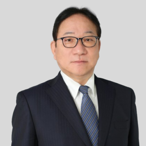
Tadahiro Suhara
TSSC
Education:
・Bachelor, Economics, Doshisha University, Japan, 1983
Experience:
・TSSC, CEO, 2023/5~
・JSR Corporation, Managing Officer, 2019~2023
・Screen Semiconductor Solutions , CEO, 2014~2019
・Dainippon Screen Manufacturing , 1983~2014
Company Profile
TSSC is a consulting company to support Semiconductor and Semiconductor Supply Chain for enabling continuous Semiconductor industry’s growth.

08:50 – 09:10
Keynote

Ken Diest
Meta
Ken Diest is a Research Manager and Tech Lead at Meta’s Reality Labs, where he leads programs focused on MEMS and micro-actuator technologies. His focus is on developing these technologies from early stage through production to address critical opto-mechanical and display challenges in AR/MR.
A Materials Scientist by training, Ken’s prior work focused on tunable devices and materials with an emphasis on optical systems. He was the editor and co-author of the book Numerical Methods for Metamaterial Design, and has previously held technology development roles at Apple, MIT Lincoln Laboratories, and Northrop Grumman that focused on new displays and nano-photonics.
Company Profile
Meta builds technologies that help people connect, find communities, and grow businesses. When Facebook launched in 2004, it changed the way people connect. Apps like Messenger, Instagram and WhatsApp further empowered billions around the world. Now, Meta is moving beyond 2D screens toward immersive experiences like augmented and virtual reality to help build the next evolution in social technology.

08:55 – 09:05
Follow the Data: Timely and Targeted
In this presentation, Mr. Sherman is excited to introduce the ISIG Chips & Wafers Data Reports for the first time to our members.
The ISIG data reports are designed as a reliable and actionable resource for semiconductor companies; providing timely and targeted data to help our members make more informed decisions.

Simi Sherman
International Semiconductor Industry Group (I.S.I.G.)
Simi Sherman is Co-Founder and CEO of Chips & Wafers, a semiconductor data and research platform, and VP of Research with ISIG.
After six years at a Buy-Side global equities Hedge Fund, where he was a Partner and led semiconductor research, Simi Co-founded Chips & Wafers. Working together with ISIG, Chips & Wafers provides semiconductor companies and investors with timely and actionable data they utilize in making more informed decisions.
Company Profile
Established in 2010, the International Semiconductor Industry Group (ISIG) is a prestigious and trusted global platform, known for fostering collaboration and driving innovation across the semiconductor industry. With a strong foundation through its International Semiconductor Executive Summits (I.S.E.S.), ISIG orchestrates influential regional summits across the U.S., Middle East, Europe and Asia, fully endorsed by local governments and leading companies throughout the semiconductor supply chain.
At ISIG, we are more than just event organizers—we serve as a catalyst for shaping the future of the semiconductor industry. Through high-level executive recruitment, expert consultation, and strategic investor engagement, ISIG empowers global collaboration, helping industry leaders connect, collaborate, and innovate. Our vision is to create a trusted network that transcends borders and disciplines, uniting government officials, academic experts, and investors to tackle the most pressing challenges and seize the greatest opportunities in the semiconductor ecosystem.
Together, we ensure the semiconductor industry remains at the forefront of technological advancement and economic growth, shaping a sustainable future for the global market.

08:55 – 09:05
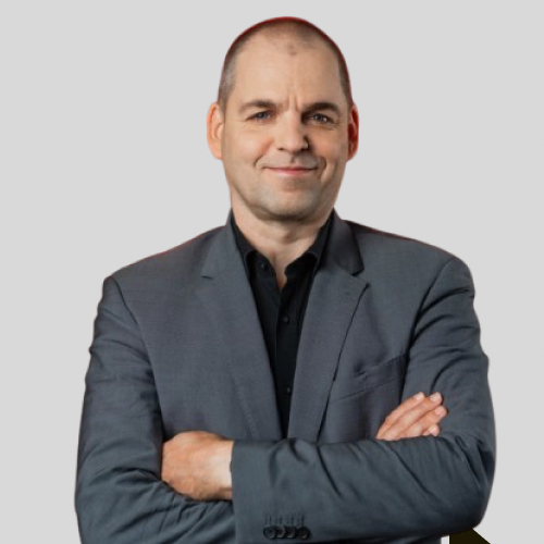
Frank Bösenberg
Silicon Saxony
08:55 – 09:15
Future of AI Hardware Enabled by Advanced Packaging
Chiplet architectures are fundamental to the continued economic viable growth of power efficiency of AI hardware and edge computing. The slowing of Moore’s law has also placed advanced packaging at the critical juncture of technology-architecture intersection driving unique product capabilities. New heterogeneous architectures like 2.5D architectures and 3D Hybrid bonded architectures driving AMD’s industry leading advanced technology roadmap to enable power, performance, area, and cost (PPAC) will be discussed. Other topics including Chiplets for AI, challenges and solutions for large chiplet modules etc. will also be discussed.
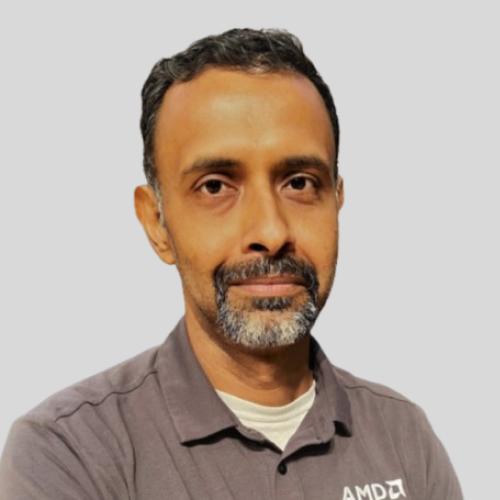
Raja Swaminathan, Ph.D.
AMD
Dr. Raja Swaminathan is the Corporate Vice President of Packaging at AMD, spearheading the development of AMD’s advanced packaging and heterogeneous integration roadmap. With a distinguished career spanning roles at Intel, Apple, and now AMD, Dr. Swaminathan’s expertise in design-technology co-optimization and dedication to optimizing power, performance, area, and cost (PPAC) have led to significant technological advancements such as EMIB, Apple’s Mx packages, 3D V-Cache, and 3.5D architectures for AI accelerators. Dr. Swaminathan holds a PhD from Carnegie Mellon University and an undergraduate degree from IIT Madras. With over 100 patents and more than 40 published papers to their name, Dr. Swaminathan was recently recognized as an IEEE Fellow and serves as a technical advisor to multiple startups. His unwavering commitment to heterogeneous integration continues to drive the boundaries of silicon technology.
Company Profile
For 50 years, AMD has driven in high-performance computing, graphics, and visualization technologies – the building blocks for gaming, immersive platforms, and the datacenter. Hundreds of millions of consumers, leading Fortune 500 businesses and cutting-edge scientific research facilities around the world rely on AMD technology daily to improve how they live, work and play. AMD employees around the world are focused on building great products that push the boundaries of what is possible. For more information about how AMD is enabling today and inspiring tomorrow, visit AMD (NASDAQ:AMD) on their website, blog, Facebook and Twitter pages.

08:55 – 09:15
Keynote: CASE STUDY (Yield): Optimizing Yield at Scale using Digital Twins
● Real-world insights on optimizing fab production while balancing efficiency

Prashanth Aprameyan
Intel Foundry
Company Profile
Intel’s systems foundry approach offers full-stack optimization from the factory network to software. Intel and its ecosystem empower customers to innovate across the entire system through continuous technology improvements, reference designs and new standards. Intel Foundry is an independent foundry business that meets our customers’ unique product needs, including our industry-leading sort and test capabilities. Whether front-end or back-end design is needed, when integrated with our foundry co-optimized development kits based on industry-standard tools and flows and powerful silicon IPs, the result is true innovation.

08:55 – 09:10
Track the Tariffs; Timely and Targeted Data
Update on Global Semiconductor Market Trends
In this presentation Mr. Sherman is excited to announce the launch of the ISIG Chips & Wafers Data Reports.
The ISIG Data reports provide timely and targeted data, used by semiconductor companies to make more informed decisions for their businesses.
Mr. Sherman will demonstrate the value of diving beyond the surface and exploring a more granular view of the available data, and show how timely tracking can help monitor the impact of global tariffs.

Simi Sherman
International Semiconductor Industry Group (I.S.I.G.)
Simi Sherman is Co-Founder and CEO of Chips & Wafers, a semiconductor data and research platform, and VP of Research with ISIG.
After six years at a Buy-Side global equities Hedge Fund, where he was a Partner and led semiconductor research, Simi Co-founded Chips & Wafers. Working together with ISIG, Chips & Wafers provides semiconductor companies and investors with timely and actionable data they utilize in making more informed decisions.
Company Profile
Established in 2010, the International Semiconductor Industry Group (ISIG) is a prestigious and trusted global platform, known for fostering collaboration and driving innovation across the semiconductor industry. With a strong foundation through its International Semiconductor Executive Summits (I.S.E.S.), ISIG orchestrates influential regional summits across the U.S., Middle East, Europe and Asia, fully endorsed by local governments and leading companies throughout the semiconductor supply chain.
At ISIG, we are more than just event organizers—we serve as a catalyst for shaping the future of the semiconductor industry. Through high-level executive recruitment, expert consultation, and strategic investor engagement, ISIG empowers global collaboration, helping industry leaders connect, collaborate, and innovate. Our vision is to create a trusted network that transcends borders and disciplines, uniting government officials, academic experts, and investors to tackle the most pressing challenges and seize the greatest opportunities in the semiconductor ecosystem.
Together, we ensure the semiconductor industry remains at the forefront of technological advancement and economic growth, shaping a sustainable future for the global market.

08:55 – 09:15
Keynote
Sensing Hope at the Edge
Machine Learning at THE EDGE. Nearly every company, investor, product launch, and presentation these days is about “ML at The Edge” as the next, great technology wave. And where there is a wave, there are riders, hoping to cash in. For me, sensors are clearly the edge, breaking the boundary between the physical and digital worlds. Driven by cost, size, power constraints, MEMS is the technology sensing the edge. And with so much data being collected, doing the analysis at the edge with ML decreases latency and saves power on data transmission. But where is the money? I’ll talk about the forces at play, large and small, and offer some experiences from MEMS at the edge. And also share my hope that beyond the hype, there is good to be done. That new understanding from all the data and algorithms will help us to leave the planet better than we found it.

Peter Hartwell, Ph.D.
TDK InvenSense
Dr. Peter G. Hartwell is VP of Engineering at TDK US Corporation driving global technology and strategy. Peter came to TDK through its acquisition of Invensense where he was the CTO. Peter has over 30 years experience commercializing silicon MEMS systems, working on sensors, actuators, and software at all levels. Prior to InvenSense, Peter was Architect of Sensing Hardware at Apple and was a Distinguished Technologist at Hewlett-Packard Labs. Peter has over 40 worldwide patents on MEMS devices and sensor applications. Peter has a B.S. in Materials Science from the University of Michigan and a Ph. D. in Electrical Engineering from Cornell University.
Company Profile
InvenSense, a TDK Group company, is a world-leading provider of sensor solutions, including MEMS and magnetic sensors for consumer, industrial, and automotive applications. InvenSense MEMS sensors are known to be best-in-class for reasons that include high performance and reliability, high-volume manufacturing capacity and supply stability, ongoing hardware and software innovation, and ultra-low power consumption. They can be found in Mobile, Wearable, Smart Home, Industrial, Automotive, IoT, and Robotics products, among others. Founded in 2003, InvenSense has a 20+ year history of patented sensor technology across Motion, Sound, and Ultrasonic solutions, including the invention of the 6-axis IMU. InvenSense is dedicated to enabling partner success and enhancing lives through sustainable sensor innovation. In May of 2017, InvenSense became part of the MEMS Sensors Business Group of TDK Corporation, based in Tokyo, Japan. InvenSense is headquartered in San Jose, California and has offices in Boston, China, Taiwan, Korea, Japan, France, Canada, Slovakia, and Italy.

Day 1 Morning Session Moderator
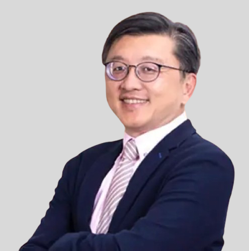
Yu-Po Wang, Ph.D.
SPIL
Yu-Po Wang received Ph.D. in Mechanical Engineering from Binghamton University, State University of New York , U.S.A.
In 1997, he started career at Gintic Institute of Manufacturing Technology in Singapore.
He joins SPIL in 1998 and leads the R&D Package Application and Technology Support Team in substrate/package design, material characterization and advanced package.
Dr. Wang has strong knowledge and experience in packaging characterization including thermal/ electrical simulation, advanced material(co-development), design and advanced packaging development. He has over 83 patents in US.
IEEE Electronics Packaging Society Board of Governors (BoG) member from 2025
IEEE Electronics Packaging Society Taipei Chapter Executive Committee from 2025

09:00 – 09:20
Opening Speech

Ministry of Economy, Trade and Industry (METI)

09:00 – 09:05
Welcome speech by Day 2 moderator

Wilson Hong
NIO
Senior Director, responsible for all HV components’ development in NIO, incl. PEU, DCDC, OBC, HV harness etc. Leading Person Award in electric vehicle industry of Anhui Province China. Over 16 years of working experience in electric drive and high voltage system, holds over 50 patents in CN, EU and US. Win the first Prize of Science and Technology Progress of China Association of Automobile Manufactures in 2021.
Company Profile
NIO is a global smart electric vehicle company. Founded in 2014, NIO has been committed to shaping a joyful lifestyle by offering high-performance smart electric vehicles and ultimate experience. NIO is the first car company listed on the NYSE, HKSE and SGX. NIO currently has two major brands under its umbrella: NIO and ONVO. Nine years into establishment, NIO is one of the leading companies in the global premium smart electric vehicle market.


Dr. Ali Amur Ali Al Shidhani
Ministry of Transport, Communications and Information Technology (MTCIT)
Company Profile
The Ministry of Transport, Communications and Information Technology supervises a number of national projects Such as, the ports and airports that connect the Sultanate with the world and contribute to diversifying the sources of income and achieve sustainable development in various economic, industrial, commercial, tourism and other fields.
These efforts are accompanied with the Ministry’s relentless strive to make the transport and logistics sectors in the Sultanate have a global reputation, to be the second source of national income and within the top ten in logistics performance at the international level by 2040.
At the local level, side by side with all these projects, The Ministry works to regulate land and sea transport industries by issuing the needed legislations.
The Ministry is also the responsible body for formulating and implementing the government digital strategies and programs in the Sultanate of Oman. Its main mission is to raise the level of efficiency in government performance, support innovation in service delivery, and enhance spending and economic growth through the use of information and communication technology.

09:00 – 09:25
Humanoid Robotics: 优必选 Ubtrobot (TBC) / 智元 (TBC)
09:00 – 09:05
Welcome Speech

Prof. Shaojun Wei
IME, Tsinghua University
Dr. Shaojun Wei is the professor of Tsinghua University; Member of the National Integrated Circuit Industry Development Advisory Committee; Vice President of China Semiconductor Industry Association (CSIA) and President of Fabless Chapter CSIA. Dr. Wei was the President & CEO of Datang Telecom Technology Co., Ltd. and the CTO of Datang Telecom Industry Group between 2001-2006.
Dr. Wei has been working on VLSI design methodologies research and reconfigurable computing technology research. He has published more than 200 peer-reviewed papers and 6 monographs. He owns more than 130 patents, including 18 US patents. Dr. Wei is the IEEE Fellow, the Fellow of Chinese Institute of Electronics (CIE), the Fellow of Asia-Pacific AI Association, and the academician of the International Eurasian Academy of Science (IEAS).
Dr. Wei had won many awards including China National Second Award for Technology Invention (2015), China National Second Award for Technology Progress (2001), SIPO & WIPO Patent Golden Award (2003, 2015), First Award for Science and Technology of Ministry of Education (2014, 2019), China, First Award for Technology Invention of CIE (2012, 2017, 2020), EETimes China IC Design Achievement Award (2018), Aspencore Outstanding Contribution Award of the Year/Global Electronic Achievement Awards (2018), SEMI Special Contribution Award (2019) and IEEE CAS Industrial Pioneer Award (2020).
Company Profile
The campus of Tsinghua University is situated in northwest Beijing on the site of the former imperial gardens of the Qing Dynasty, and surrounded by a number of historical sites.
Tsinghua University was established in 1911, originally under the name “Tsinghua Xuetang”. The school was renamed “Tsinghua School” in 1912. The university section was founded in 1925. The name “National Tsinghua University” was adopted in 1928.
The faculty greatly valued the interaction between Chinese and Western cultures, the sciences and humanities, the ancient and modern. Tsinghua scholars Wang Guowei, Liang Qichao, Chen Yinque and Zhao Yuanren, renowned as the “Four Tutors” in the Institute of Chinese Classics, advocated this belief and had a profound impact on Tsinghua’s later development.
Tsinghua University was forced to move to Kunming and join with Peking University and Nankai University to form the Southwest Associated University due to the Resistance War against the Japanese Invasion in 1937. In 1946 The University was moved back to its original location in Beijing after the war.
After the founding of the People’s Republic of China, the University was molded into a polytechnic institute focusing on engineering in the nationwide restructuring of universities and colleges undertaken in 1952. In November 1952, Mr. Jiang Nanxiang became the President of the University. He made significant contributions in leading Tsinghua to become the national center for training engineers and scientists with both professional proficiency and personal integrity.
Since China opened up to the world in 1978, Tsinghua University has developed at a breathtaking pace into a comprehensive research university. At present, the university has 20 schools and 59 departments with faculties in science, engineering, humanities, law, medicine, history, philosophy, economics, management, education and art.
With the motto of “Self-Discipline and Social Commitment” and the spirit of “Actions Speak Louder than Words”, Tsinghua University is dedicated to the well-being of Chinese society and to world development. As one of China’s most prestigious and influential universities, Tsinghua is committed to cultivating global citizens who will thrive in today’s world and become tomorrow’s leaders. Through the pursuit of education and research at the highest level of excellence, Tsinghua is developing innovative solutions that will help solve pressing problems in China and the world.

09:00 – 09:10
Opening Videos 宣传片播放
09:00 – 09:35
Registration
09:00 – 09:20
Keynote
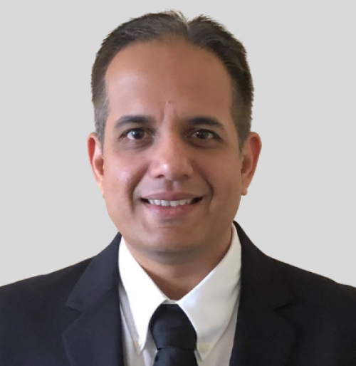
Rahul Manepalli, Ph.D.
Intel Corporation
Rahul Manepalli is an Intel Fellow and Sr. Director of Module Engineering in the Substrate Package Technology Development Organization in Intel. Rahul and his team are responsible for developing next generation of materials, processes and equipment for Intel’s package pathfinding and development efforts. His team has been the driving force behind many of the technology innovations in Intel’s Embedded Multi-die Interconnect Bridge (EMIB) and other substrate technologies. Rahul has also had an instrumental role in leading Intel’s assembly materials development and pathfinding efforts leading to several innovations in encapsulants, thermal interface materials and solder alloys. Rahul is the author of over 100 patent publications in semiconductor packaging, over 50 technical papers and invited talks and has a Ph.D. in Chemical Engineering from the Georgia Institute of Technology.
Company Profile
Intel (Nasdaq: INTC) is an industry leader, creating world-changing technology that enables global progress and enriches lives. Inspired by Moore’s Law, we continuously work to advance the design and manufacturing of semiconductors to help address our customers’ greatest challenges. By embedding intelligence in the cloud, network, edge and every kind of computing device, we unleash the potential of data to transform business and society for the better.
To learn more about Intel’s innovations, go to newsroom.intel.com and intel.com.

09:00 – 09:20
Keynote
We power AI: High density solutions for AI accelerators
In today’s rapidly evolving technological landscape, the demand for cutting-edge Artificial Intelligence (AI) solutions has never been greater. At the heart of these innovations lies an often-overlooked yet crucial component: power. As a leader in the semiconductor industry, we are at the forefront of powering AI from grid to core. This approach ensures that every stage of the power conversion process is optimized to meet the stringent demands of AI data centers. Enabling efficient power conversion from grid to core is essential for achieving superior power densities, thereby enhancing performance/watt while reducing the total cost of ownership (TCO). In this talk, we will focus on the final power conversion step, specifically the second stage down to the core voltage. Our power modules, which enable true vertical power delivery, significantly reduce power delivery network losses, thereby increasing overall system efficiency. Infineon high density solutions push the power density envelope without compromising thermal performance. Additionally, we will talk about our new quad module and demonstrate the benefits of its vertical power flow through chip embedding.
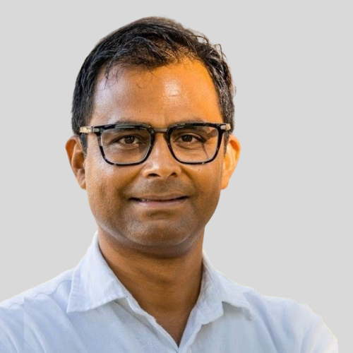
Athar Zaidi
Infineon Technologies AG
Athar Zaidi is a SVP/GM at Infineon Technologies where he manages Power ICs and Connectivity Systems (PCS) Business Line under Power and Sensor Systems (PSS) Division. Athar joined Infineon in 2016, prior to that he held leadership positions at Dialog Semiconductors, Maxim Integrated and Semtech Corporation where he managed global semiconductor businesses focusing on power management in Enterprise, Consumer, Industrial, Telecom and Automotive space. Athar has an MBA from UC Berkeley and Dual MS in Mechanical and Computer Engineering from North Carolina State University.
Company Profile
Here at Infineon, we combine entrepreneurial success with responsible action to make life easier, safer, and greener. Barely visible, semiconductors have become an indispensable part of everyday life. We play a key role in shaping a better future – with microelectronics that link the real and the digital world. Our semiconductors enable efficient energy management, smart mobility, as well as secure, seamless communications in an increasingly connected world. Infineon designs, develops, manufactures and markets a broad range of semiconductors and system solutions. The focus of its activities is on automotive and industrial electronics, communication and information technologies, IoT, sensor technology and security. The product range comprises standard components, software, customer-specific solutions for devices and systems, as well as specific components for digital, analog, and mixed-signal applications.

09:05 – 09:20
Welcome and Product speech

Gerald Yin, Ph.D.
AMEC
Company Profile
Advanced Micro-Fabrication Equipment Inc. China (AMEC, stock code: 688012) is an innovative Asia-based semiconductor equipment company with a range of proprietary fabrication solutions designed to advance technology, increase productivity, and reduce manufacturing costs for leading global manufacturers of semiconductors and LEDs. Headquartered in Shanghai, the company is an entrenched supplier of dielectric and TSV etch tools, helping chipmakers build devices at process nodes as low as 5nm and beyond. In addition, AMEC’s MOCVD system has become a market leader in China for producers of LEDs and power devices. AMEC products are used today by technology leaders in Chinese mainland and Taiwan region, as well as Singapore, Korea, Germany, Italy and so on.

09:10 – 09:40
Future Packaging/System Challenges for AI Data Centers
Artificial Intelligence is the largest technology transformation since Internet revolutionized communication and business. This transformation has required advancement in Si, Memory, Packaging, and System technologies. In this talk, the packaging and system technology challenges will be presented.
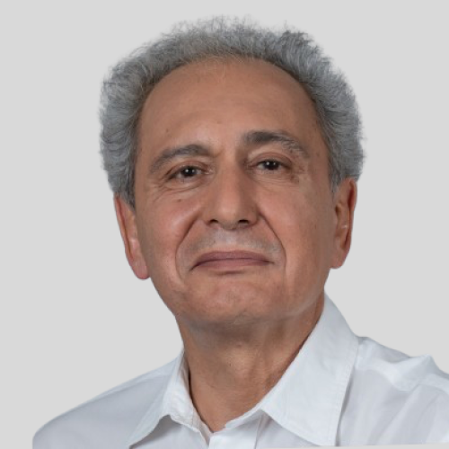
Babak Sabi, Ph.D.
AWS Annapurna Labs
Dr. Babak Sabi is VP of Technology at AWS/Annapurna Lab. Babak joined AWS in 2024 after 40 years in Intel. Babak was Senior Vice President and the General Manager of Assembly & Test Technology Development (ATTD) at Intel Corporation. Since 2009, he has been responsible for the company’s packaging, assembly, and test process technology development. During Babak’s tenure in ATTD 2.5D and 3D Advanced Packages were developed and ramp to high Volume Manufacturing. Additionally ATTD team made many advancement in Substrate and Test Technology.
Prior to leading ATTD, Babak oversaw Intel’s Corporate Quality Network from 2002 to 2009 where he led product reliability, customer satisfaction and quality business practices.
Babak joined Intel in 1984 after receiving Babak his Ph.D. in solid state electronics from Ohio State University in 1984.
Company Profile
Launched in 2006, Amazon Web Services (AWS) began exposing key infrastructure services to businesses in the form of web services — now widely known as cloud computing. The ultimate benefit of cloud computing, and AWS, is the ability to leverage a new business model and turn capital infrastructure expenses into variable costs. Businesses no longer need to plan and procure servers and other IT resources weeks or months in advance. Using AWS, businesses can take advantage of Amazon’s expertise and economies of scale to access resources when their business needs them, delivering results faster and at a lower cost.
Today, Amazon Web Services provides a highly reliable, scalable, low-cost infrastructure platform in the cloud that powers hundreds of thousands of businesses in 190 countries around the world. With data center locations in the U.S., Europe, Singapore, and Japan, customers across all industries are taking advantage of our low cost, elastic, open and flexible, secure platform.

09:10 – 09:30
Keynote

Gustav Kalbe
EU Commission
Company Profile
The European Commission is the EU’s politically independent executive arm. The Directorate‑General for Communications Networks, Content and Technology is the Commission department responsible to develop a digital single market to generate smart, sustainable and inclusive growth in Europe.
Follow the latest EU tech news on Twitter, Facebook, Instagram and YouTube via @DigitalEU.

09:10 – 09:30
Global Semiconductor Overview & Landscape Understanding
Salah Nasri
I.S.E.S.
Salah Nasri is the CEO & Co-Founder of the International Semiconductor Executive Summits (ISES), a division of the International Semiconductor Industry Group Ltd. an influential organization within the semiconductor industry. With extensive experience in the sector, Nasri has played a pivotal role in fostering global collaboration among semiconductor leaders. Under his leadership, ISES has become a premier platform for industry executives to connect, share insights, and drive innovation across various regions including the United States, Europe, Asia, and the Middle East.
Salah Nasri has been instrumental in expanding the reach and impact of ISES, organizing significant events that bring together decision-makers from across the semiconductor ecosystem. These events provide opportunities for networking, collaboration, and the exchange of ideas crucial for advancing the industry in areas such as semiconductor manufacturing, MEMS, AI, automotive electronics, and more.
His leadership has not only enhanced the visibility of ISES globally but also strengthened partnerships with key industry players, ensuring that ISES remains at the forefront of semiconductor innovation and development. Salah Nasri has previously worked at Goldman Sachs’s, Credit Suisse and International Business Development Group. Salah Nasri graduated from Oxford University and Loughborough University in International Relations and Economics. In 2024, Salah Nasri became a Stanford University Alumni after completing the Stanford Executive Program.
Company Profile
Established in 2010, the International Semiconductor Industry Group (I.S.I.G.) is a prestigious and trusted association within the semiconductor industry, renowned for orchestrating major regional summits across the globe, ranging from the U.S, the Middle East & Asia via our division, the International Semiconductor Executive Summits (I.S.E.S.). Our summits, are fully endorsed by local governments and leading companies in all areas of the semiconductor supply chain.
Moreover, I.S.E.S. serves as the Premier platform for senior executives in technology, manufacturing, and R&D from diverse semiconductor companies, technology providers, and affiliated industries. Our events are instrumental helping to shed light onto key industry trends, drive innovation and influence key decisions to help shape, and advance the growth of the semiconductor sector. Join us today!

09:10 – 09:15
Introduction of Government Officials and VIPs 介绍与会领导 及嘉宾
09:10 – 09:30
Keynote
AI Inspired. Systems Accelerated.
The shifting landscape of technology requires a multi-faceted foundry approach to keep pace with increasing workload of data centers and high-performance computing (HPC) systems. The use of chiplets and “system of chips” offer a way to unlock exponential improvements in semiconductor products. Intel Foundry is addressing these needs with decades of experience in world class manufacturing, innovative advancements in packaging and system technology optimization, delivered through a more resilient and more sustainable global supply chain. Join us as we outline how Intel Foundry is tackling the next wave of semiconductor breakthroughs.

Kevin O’Buckley
Intel Foundry
Kevin O’Buckley is senior vice president and general manager of Foundry Services at Intel Corporation. In this role, he is responsible for driving continued growth for Intel Foundry and its differentiated systems foundry offerings, which go beyond traditional wafer fabrication to include packaging, chiplet standards and software, as well as U.S.- and Europe-based capacity.
Prior to joining Intel, O’Buckley was senior vice president of Marvell’s Compute and Custom Solutions Engineering teams, developing advanced technology chips for infrastructure applications including artificial intelligence and machine learning, 5G wireless, and data center compute and networking. While at Marvell he also served as senior vice president and general manager of the company’s ASIC business, and he was a member of the board of directors at Marvell Government Solutions, developing semiconductor solutions for aerospace and defense customers.
O’Buckley joined Marvell as part of its 2019 acquisition of Avera Semiconductor, where he served as chief executive. He has also held various executive engineering and business leadership roles at Global Foundries and at IBM, where he served for more than 17 years leading technology development and manufacturing organizations.
Company Profile
Intel’s systems foundry approach offers full-stack optimization from the factory network to software. Intel and its ecosystem empower customers to innovate across the entire system through continuous technology improvements, reference designs and new standards. Intel Foundry is an independent foundry business that meets our customers’ unique product needs, including our industry-leading sort and test capabilities. Whether front-end or back-end design is needed, when integrated with our foundry co-optimized development kits based on industry-standard tools and flows and powerful silicon IPs, the result is true innovation.

09:15 – 09:40
Welcome Address * 3 领导致辞
09:15 – 09:45
Keynote
The New Era in Si Photonics
AI has been extending its influence in nearly every aspect of our daily endeavors; but, the power consumption seems to be the accompanied pain as the industry continue to push for ever- increasing computing power.
Over the years, among other things, Si Photonics has been heralded as a breakthrough in power saving.
However, so far, it appears to lack large volume production for >100G optical solution.
The debut of the 200G CPO with MRM is the watershed for the new era in Si photonics.
This presentation will address the driving force of the new era along with the illustration of critical aspects in Si photonics device manufacturing, followed by the introduction of technology platforms that are intended to power the AI acceleration.
C.S. Yoo, Ph.D
TSMC
C.S. is a 30+ years’ veteran of semiconductor industry.
Ever since joined TSMC, he has been working in various technology R&D fields and Operations.
He took various managerial positions in RD Process Module, SRAM, DRAM and Embedded DRAM.
CS also led TSMC Mask RD and Operation Division before taking the position of VP in Specialty Technology RD.
CS received his PhD in Chemical Engineering from WPI (Worcester Polytechnic Institute)
Company Profile
TSMC pioneered the pure-play foundry business model when it was founded in 1987, and has been the world’s leading dedicated semiconductor foundry ever since. The Company supports a thriving ecosystem of global customers and partners with the industry’s leading process technologies and portfolio of design enablement solutions to unleash innovation for the global semiconductor industry. With global operations spanning Asia, Europe, and North America, TSMC serves as a committed corporate citizen around the world.
TSMC deployed 288 distinct process technologies, and manufactured 11,878 products for 522 customers in 2024 by providing the broadest range of advanced, specialty and advanced packaging technology services. The Company is headquartered in Hsinchu, Taiwan. For more information please visit https://www.tsmc.com.

09:15 – 10:15
Networking Coffee Break & Business Meetings
09:15 – 09:35
Keynote

Christina Strohrmann, Ph.D.
Bosch Sensortec
Dr. Christina Strohrmann is an engineering director and thought leader in advanced sensor technologies, currently serving as Director of Engineering Advanced Products at Bosch Sensortec. With over a decade of experience spanning MEMS, TMR, optical sensors, and AI-driven product development, she is responsible for technology management and leading cross-functional teams from early-stage innovation to mass production. Named an “Emerging Leader” by the SEMI MEMS & Sensors Industry Group, she combines deep technical expertise with strategic vision, having driven groundbreaking advancements in dual-core sensors, automated data pipelines, and smart sensing for consumer electronics.
Company Profile
Bosch Sensortec is a wholly owned subsidiary of the Bosch Group, dedicated to developing and marketing a comprehensive portfolio of microelectromechanical systems (MEMS)-based sensors and solutions for consumer electronics. Headquartered in Reutlingen, Germany, the company was founded in 2005 and has since become a global leader in MEMS sensor innovation. Bosch Sensortec’s product offerings include motion sensors, environmental sensors, smart sensors, and software solutions that power a wide range of devices such as smartphones, wearables, drones, and IoT applications.
By leveraging Bosch’s decades of experience and leadership in automotive MEMS sensor technology, Bosch Sensortec brings industrial-grade performance to the consumer market. With a focus on miniaturization, energy efficiency, and intelligent sensing, the company enables smart, connected devices that respond to their environments with precision and reliability. Through continuous innovation and a strong global network, Bosch Sensortec plays a pivotal role in advancing next-generation sensor technologies for an increasingly digital and mobile world.

09:20 – 09:40
Future Packaging/System Challenges for AI Data Centers
Artificial Intelligence is the largest technology transformation since Internet revolutionized communication and business. This transformation has required advancement in Si, Memory, Packaging, and System technologies. In this talk, the packaging and system technology challenges will be presented.

Babak Sabi, Ph.D.
AWS Annapurna Labs
Dr. Babak Sabi is VP of Technology at AWS/Annapurna Lab. Babak joined AWS in 2024 after 40 years in Intel. Babak was Senior Vice President and the General Manager of Assembly & Test Technology Development (ATTD) at Intel Corporation. Since 2009, he has been responsible for the company’s packaging, assembly, and test process technology development. During Babak’s tenure in ATTD 2.5D and 3D Advanced Packages were developed and ramp to high Volume Manufacturing. Additionally ATTD team made many advancement in Substrate and Test Technology.
Prior to leading ATTD, Babak oversaw Intel’s Corporate Quality Network from 2002 to 2009 where he led product reliability, customer satisfaction and quality business practices.
Babak joined Intel in 1984 after receiving Babak his Ph.D. in solid state electronics from Ohio State University in 1984.
Company Profile
Launched in 2006, Amazon Web Services (AWS) began exposing key infrastructure services to businesses in the form of web services — now widely known as cloud computing. The ultimate benefit of cloud computing, and AWS, is the ability to leverage a new business model and turn capital infrastructure expenses into variable costs. Businesses no longer need to plan and procure servers and other IT resources weeks or months in advance. Using AWS, businesses can take advantage of Amazon’s expertise and economies of scale to access resources when their business needs them, delivering results faster and at a lower cost.
Today, Amazon Web Services provides a highly reliable, scalable, low-cost infrastructure platform in the cloud that powers hundreds of thousands of businesses in 190 countries around the world. With data center locations in the U.S., Europe, Singapore, and Japan, customers across all industries are taking advantage of our low cost, elastic, open and flexible, secure platform.

09:20 – 09:40
Keynote
Sensors and Systems in an AI first world
It seems that everything today is an AI first device, but what does this mean? In this talk I will discuss some of the ways that AI is impacting how Google thinks about our hardware devices and the components within. I will talk through some of the growing systems level considerations for number of sensors, quality and precision of measurements as well as how compute is distributed to handle the various AI models that exist. The goal will be to give the audience an overview of what exists today as well as some possibilities of how they can help shape devices of tomorrow.

Michael Pate, Ph.D.
Dr. Michael Pate received advanced degrees from Texas Tech University and Denmark Technical University concentrating in the design of Class-D amplifiers for audio systems. After completing his Ph.D. work he began at Texas Instruments where he led the design of some of the highest power integrated Class-D amps on the market. From there Dr Pate moved to product definition roles at Cirrus Logic, Audience and Knowles Electronics where he focused on mixed signal audio, DSP and algorithms and MEMS microphones respectively. He now works at Google as the Director of Audio Technology Development where his team builds experiences like Active Noise Cancellation, Audio Magic Eraser, Clear Calling and many more.
Company Profile
A problem isn’t truly solved until it’s solved for all. Googlers build products that help create opportunities for everyone, whether down the street or across the globe. Bring your insight, imagination and a healthy disregard for the impossible. Bring everything that makes you unique. Together, we can build for everyone.

09:20 – 09:40
Keynote
Terushi Shimizu
Sony Semiconductor

09:20 – 09:40
I.S.I.G. 15th Year Anniversary Welcome Speech

Salah Nasri
International Semiconductor Industry Group (I.S.I.G.)
Salah Nasri leads the International Semiconductor Industry Group, founded in 2010, it is a global leading semiconductor association known for its flagship platforms (The International Semiconductor Executive Summits), uniting top executives, government officials, researchers, and investors from around the globe to address challenges and opportunities in chip manufacturing and technology innovation. He guides the association in shaping crucial industry dialogues—ranging from trade regulations to cutting-edge chip design—and fosters collaborations that drive the future of the semiconductor sector. Salah studied International Relations and Economics at Oxford University, Loughborough University and in 2024 graduated from the Stanford Graduate School of Business Executive Program.
Company Profile
Established in 2010, the International Semiconductor Industry Group (ISIG) is a prestigious and trusted global platform, known for fostering collaboration and driving innovation across the semiconductor industry. With a strong foundation through its International Semiconductor Executive Summits (I.S.E.S.), ISIG orchestrates influential regional summits across the U.S., Middle East, Europe and Asia, fully endorsed by local governments and leading companies throughout the semiconductor supply chain.
At ISIG, we are more than just event organizers—we serve as a catalyst for shaping the future of the semiconductor industry. Through high-level executive recruitment, expert consultation, and strategic investor engagement, ISIG empowers global collaboration, helping industry leaders connect, collaborate, and innovate. Our vision is to create a trusted network that transcends borders and disciplines, uniting government officials, academic experts, and investors to tackle the most pressing challenges and seize the greatest opportunities in the semiconductor ecosystem.
Together, we ensure the semiconductor industry remains at the forefront of technological advancement and economic growth, shaping a sustainable future for the global market.

09:20 – 09:40
Reserved for Ibiden
Ahmad Bahai, Ph.D.
Texas Instruments
Dr. Ahmad Bahai is the Senior Vice President and Chief Technology Officer (CTO) at Texas Instruments, where he leads groundbreaking innovation, corporate research, and Kilby Labs.
He also serves as a Professor of the Practice at the Massachusetts Institute of Technology (MIT), is an IEEE Fellow, and is a member of the Industrial Advisory Committee for the CHIPS Act. Previously, Dr. Bahai contributed to the President’s Council of Advisors on Science and Technology’s semiconductor working group. From 2017 to 2022, he was an Adjunct Professor at Stanford University and, from 2001 to 2010, a Professor in Residence at UC Berkeley.
Dr. Bahai’s technology leadership experience includes roles as Director of Research Labs and CTO at National Semiconductor, Technical Manager of a research group at Bell Laboratories, and Founder of Algorex, a communications and acoustic IC and systems company acquired by National Semiconductor.
He has authored over 80 publications in IEEE/IEE journals and holds more than 40 patents related to systems and circuits. Dr. Bahai earned a Master of Science in Electrical Engineering from Imperial College, University of London, and a Ph.D. in Electrical Engineering from the University of California, Berkeley.
Company Profile
Texas Instruments is a global semiconductor leader focused on designing and manufacturing analog and embedded processing chips that drive electronics everywhere. With over 90 years of innovation, Tl is powering industries across automotive, industrial, communications, and personal electronics.
As part of its commitment to energy efficiency and performance, Tl is advancing Gallium Nitride (GaN) power solutions to enable smaller, faster, and more efficient systems GaN technology allows for higher power density and switching frequencies compared to traditional silicon-based power devices, making it ideal for next-generation electric vehicles,renewables, data centers, and industrial applications.
In 2024, Tl announced expanded GaN manufacturing capabilities at its Richardson, Texas facility, where it will now produce both GaN and silicon semiconductors on a single 300mm wafer line. This investment strengthens TI’s position as a fully integrated GaN supplier — from design to fabrication — ensuring quality, supply assurance, and performance leadership.
With decades of manufacturing excellence and a focus on advancing power electronics, Texas Instruments is helping to engineer a more sustainable and connected future through GaN innovation.

09:30 – 09:50
eVTOL marketing trend
ChinaeroSpace 鸿鹏航空
09:30 – 10:00
Why “Middle East” – GSME’s Journey in Search of New Talent & Hub for Semiconductor Design & Manufacturing
Semiconductors are the backbone of 4th industrial revolution enabling us to live in a smart & connected world. Connected world, Digitizing Auto Industry, social-media revolution, industrial automation, & AI decision making is spiking the demand of Integrated Circuits. Now when semiconductors are becoming the new “Oil”, fight over its control is also getting intense. Trade-war between US & China is drifting to become China-vs-West issue to gain controls over semiconductor manufacturing market. Semiconductor industry is experiencing shortage of skilled engineers in the field of microelectronics, IC design & manufacturing. GSME started its efforts over a year ago to identify & establish new hubs to support semiconductor ecosystem. GCC countries in Middle East can play a significant role in filling in the gap industry is experiencing.

Farhat Jahangir
GS Microelectronics
Farhat serves as the CEO at GS Microelectronics. Prior to joining GSME he was serving as VP & GM of Manufacturing at Onsemi, where he was managing ON Semiconductor’s largest 300mm Fab in East-Fishkill, New York for over two years. Farhat joined ON Semiconductor through Quantenna Communication acquisition in March 2019 where he was serving as SVP of Manufacturing, Operations & Quality for six plus years. Farhat played a pivotal role in making Quantenna successful through manufacturing optimization, process & yields improvements, cost reductions, & significant margins improvement. Farhat’s efforts enabled Quantenna’s successful IPO in October 2016.
Farhat has over 25 years of successful experience in global manufacturing, Fab & OSAT operations, supplier management, building partnerships, and the assurance of quality & reliability processes. Prior to joining ON Semi/Quantenna Communications, he headed semiconductor manufacturing operations and quality functions at Synerchip Corporation (acquired by Silicon Image) & SiTime (a MEMS based timing solution company). His contributions towards building and restructuring company’s lower margin product lines to higher margins, enabled market penetration and corporate margins growth in the companies he served. Farhat also held various engineering and management positions in the areas of semiconductor manufacturing in companies like Texas Instruments, Cypress Semiconductor, Silicon Image & IDT.
Farhat holds a Master of Science degree in Electrical Engineering from University of Arkansas at Fayetteville.

Maryam Al-Bulushi
GS Microelectronics


Ammar Al-Kalbani
GS Microelectronics


Ammar Al-Kalbani
GS Microelectronics

End of content
End of content