27-28 August 2025
Suwon
12:25 – 13:25
Networking Session & Exhibitor Visits, Lunch
12:25 – 12:45

Kees Wesdorp, Ph.D.
XIVER Mems Foundry
Kees Wesdorp is CEO of DeepHealth, where he leads the development of AI-driven diagnostic platforms transforming radiology and digital health. He also chairs the board at Xiver, Europe’s leading independent MEMS foundry, enabling next-generation technologies for healthtech, photonics, automotive, and industrial applications. Earlier in his career, Kees played a key role in the transformation of NXP Semiconductors, driving global operations and product innovation. He later held executive roles at Philips, leading its Precision Diagnosis division, and at Hellman & Friedman, supporting portfolio value creation. Kees holds a PhD in experimental atomic physics from Vrije Universiteit Amsterdam.
Company Profile
XIVER – More than a MEMS Foundry, leveraging a legacy of innovation
XIVER is a leading independent MEMS foundry specialized in process development, industrialization, and manufacturing of thin-film and MEMS devices.
Empowered by a team of over 110 highly skilled professionals, XIVER leverages decades of innovation and expertise from its Philips heritage.
Utilizing proven process technologies and key-enabling IP-backed platforms, XIVER delivers tailored solutions to its customers active in various markets and applications, including Industrial, Medical, Photonics, and Automotive.
With commitment to excellence, XIVER enables seamless transitions from development to medium-volume production on 200mm wafers, operating in a 2,650m2 cleanroom.
Located at the High Tech Campus Eindhoven, the Netherlands, XIVER is the only independent, pure-play MEMS foundry in Europe, serving customers globally.
Company Products & Services
XIVER offers innovative product platform solutions, such as its cutting-edge CMUT ultrasound platform that powers the next generation of interventional, portable point-of-care, and wearable ultrasound imaging devices. Our streamlined process ensures innovative, high-performance MEMS solutions tailored to your needs.
We employ a phase-gated approach to ensure a predictable and reliable path for MEMS processes, from concept to manufacturing.

12:30 – 12:40
Choon Khoon Lim
ASMPT Limited
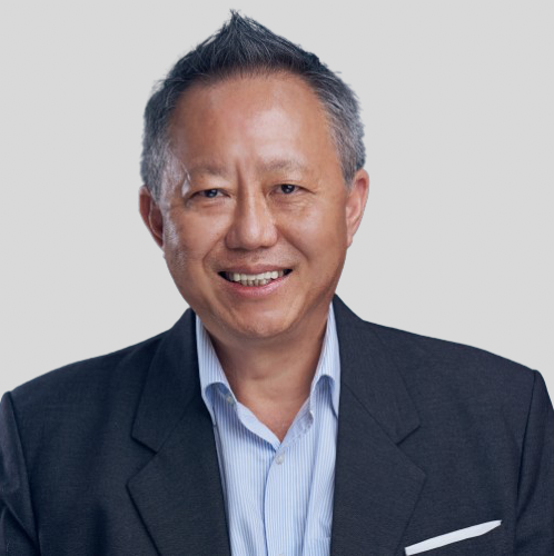
LIM Choon Khoon (CK) is a Senior Vice President and Chief Executive Officer of Semiconductor Solutions Advanced Packaging (AP).
CK’s career spans key engineering, manufacturing, and regional functional and global general management roles with several global semiconductor companies. As Chief Executive Officer of the Segment’s AP Business Group, he helps provide the industry’s leading first-level interconnect technologies covering leading AP First Level Interconnect (FLI) technologies for logic, HBM, Si Photonics & Co-Packaged Optics, wafer die singulation solution for advanced fabricated wafers and Panel ECD for fine Line/Space organic and glass substrate & Wafer PVD, that are well-positioned to serve and to scale with the most demanding AP needs.
CK holds a Bachelor of Science (Honours) in Production Engineering and Production Management degree from the University of Nottingham, United Kingdom
Company Profile
ASMPT, founded in 1975, is headquartered in Singapore and is listed in Hong Kong Stock Exchange since 1989.
ASMPT is the only company in the world that offers high-quality equipment for all major steps in the electronics manufacturing process – from carrier for chip interconnection to chip assembly and packaging to SMT. No other supplier offers a comparable range and depth of process expertise.
Semiconductor Solutions Segment Business of ASMPT offers a diverse product range from bonding to molding and trim & form to the integration of these activities into complete in-line systems for the microelectronics, semiconductor, camera modules, advanced packaging, photonics, and optoelectronics industries.
The group has successfully established itself as the leading player in the back-end assembly and packaging market with its innovative solutions and constant focus on customer value creation.

12:35 – 13:35
Buffet Lunch
12:35 – 13:40
Lunch Break
12:40 – 14:00
Lunch Break
12:40 – 12:50

ATLANT 3D
Company Profile
ATLANT 3D has mastered control of matter at the atomic scale, ushering in a new era in manufacturing. For research teams and manufacturers working at the frontiers of technology, we’ve created what was once thought unattainable: a system that builds materials and devices, atom by atom, with unprecedented precision and speed.
While others are constrained by traditional manufacturing limits, our breakthrough technology makes it possible to create the seemingly impossible, from next-generation quantum computers to devices that can operate in the harsh conditions of space. By replacing complex, resource-heavy processes with precise atomic-scale fabrication, we’re transforming technology while making manufacturing sustainable. We’re providing innovative teams the power to build technologies today that will define tomorrow’s world, using fewer resources to achieve greater possibilities.
Based in Copenhagen and London, with operations in the US, ATLANT 3D partners with research institutions and industrial companies to expand the boundaries of technological possibility.
Company Products & Services
ATLANT 3D is redefining microfabrication with its patented Direct Atomic Layer Processing (DALP®) technology. Our NANOFABRICATOR™ platform enables localized atomic layer processing for rapid material discovery, prototyping, and scalable device fabrication—bridging the gap from lab to fab.
Beyond hardware, we offer Pilot Projects and Joint Development Services to validate new materials and device architectures. A-HUB, our Microfabrication-as-a-Service (MaaS) centre, provides R&D teams with atomic-scale precision without the need for costly infrastructure.
From concept to fabrication, ATLANT 3D partners with academia and industry to drive next-generation innovations beyond conventional limits.

12:50 – 13:50
Buffet Lunch
12:50 – 13:35
PANEL (Time): Smart Fabs & the Future Workforce

Panelist
Reserved
GlobalFoundries
Company Profile
GF is one of the world’s leading semiconductor manufacturers and the only one with a truly global footprint. We are redefining innovation and semiconductor manufacturing by developing feature-rich process technology solutions that provide leadership performance in pervasive high growth markets. As a steadfast partner, with a unique mix of design, development and fabrication services, GF works collaboratively alongside our customers to bring a broad range of innovative products to market. With a global customer base, a talented and diverse workforce and an at-scale manufacturing footprint spanning three continents, GF is delivering a new era of more.


Panelist
Reserved NXP
NXP Semiconductors
Company Profile
NXP Semiconductors N.V. (NASDAQ: NXPI) brings together bright minds to create breakthrough technologies that make the connected world better, safer and more secure. As a world leader in secure connectivity solutions for embedded applications, NXP is pushing boundaries in the automotive, industrial & IoT, mobile, and communication infrastructure markets while delivering solutions that advance a more sustainable future. Built on more than 60 years of combined experience and expertise, the company has approximately 34,200 team members in more than 30 countries and posted revenue of $13.28 billion in 2023. Find out more at www.nxp.com.


Panelist
Reserved
Infineon Technologies AG
Company Profile
Here at Infineon, we combine entrepreneurial success with responsible action to make life easier, safer, and greener. Barely visible, semiconductors have become an indispensable part of everyday life. We play a key role in shaping a better future – with microelectronics that link the real and the digital world. Our semiconductors enable efficient energy management, smart mobility, as well as secure, seamless communications in an increasingly connected world. Infineon designs, develops, manufactures and markets a broad range of semiconductors and system solutions. The focus of its activities is on automotive and industrial electronics, communication and information technologies, IoT, sensor technology and security. The product range comprises standard components, software, customer-specific solutions for devices and systems, as well as specific components for digital, analog, and mixed-signal applications.


Panelist
onsemi
Company Profile
onsemi (Nasdaq: ON) is driving disruptive innovations to help build a better future. With a focus on automotive and industrial end-markets, the company is accelerating change in megatrends such as vehicle electrification and safety, sustainable energy grids, industrial automation, and 5G and cloud infrastructure. With a highly differentiated and innovative product portfolio, onsemi creates intelligent power and sensing technologies that solve the world’s most complex challenges and leads the way in creating a safer, cleaner, and smarter world.

12:55 – 14:10
Lunch Break
13:05 – 14:00
Panel Session: How Silicon Photonics is set to transform interconnect architecture for AI

Moderator
Kevin Soukup
GlobalFoundries
Kevin Soukup is Senior Vice President of Silicon Photonics Product Line at GF, a position he was appointed to in 2024. In this role, Mr. Soukup leads the company’s Silicon Photonics business that enables customers to transport enormous volumes of data through high-speed, power efficient electro-optical systems.
Prior to his current role, he served as Chief Strategy Officer developing the company’s integrated strategy and ensuring that GF has the management systems in place to deliver. Mr. Soukup joined GF in 2011 and held positions of increasing responsibility in technology development and manufacturing operations for the next seven years. In 2018, Kevin transitioned to VP of Business Transformation and helped prepare GF for IPO in 2021.
Before his career with GF, Mr. Soukup spent eleven years with Samsung Electronics’ semiconductor unit in engineering and operations management positions.
Mr. Soukup holds a Bachelor of Science in Chemical Engineering from the University of Florida. He currently serves as a member of the board of directors of VueReal.
Company Profile
GF is one of the world’s leading semiconductor manufacturers and the only one with a truly global footprint. We are redefining innovation and semiconductor manufacturing by developing feature-rich process technology solutions that provide leadership performance in pervasive high growth markets. As a steadfast partner, with a unique mix of design, development and fabrication services, GF works collaboratively alongside our customers to bring a broad range of innovative products to market. With a global customer base, a talented and diverse workforce and an at-scale manufacturing footprint spanning three continents, GF is delivering a new era of more.


Panelist
Near Margalit, Ph.D.
Broadcom
Dr. Near Margalit has held several executive positions in the optical connectivety industry. He founded Zaffire Inc., a metro DWDM Optical Networking company before moving on to lead Source Photonics as CEO from 2002-2013, growing the company to one of the premier optical transceiver vendors. He was the CTO and Head of Product Development for Intel’s Silicon Photonics for the commercial introduction of Silicon Photonics in 2015-2016. From 2018 to present he has been with the Optical Systems Division of Broadcom where he is currently the VP and General Manager of the division. He holds a Ph.D in Optoelectronics from UC Santa Barbara and a B.S. in Applied Physics from CalTech.
Company Profile
Broadcom Inc. designs, develops, and markets digital and analog semiconductors. The Company offers wireless RF components, storage adapters, controllers, networking processors, switches, fiber optic modules, motion control encoders, and optical sensors. Broadcom markets its products worldwide.

Panelist
M. Ashkan Seyedi, Ph.D.
NVIDIA
Ashkan Seyedi received a dual bachelor’s in electrical and computer engineering from the University of Missouri-Columbia and a Ph.D. from University of Southern California working on photonic crystal devices, high-speed nanowire photodetectors, efficient white LEDs, and solar cells. With a decade of industry experience at Intel, Hewlett Packard Enterprise and now NVidia, Dr. Seyedi has been working on developing high-bandwidth, efficient optical interconnects for exascale, and high-performance computing applications.
Company Profile
Since its founding in 1993, NVIDIA (NASDAQ: NVDA) has been a pioneer in accelerated computing. The company’s invention of the GPU in 1999 sparked the growth of the PC gaming market, redefined computer graphics, ignited the era of modern AI and is fueling the creation of the metaverse. NVIDIA is now a full-stack computing company with data-center-scale offerings that are reshaping industry.


Panelist
Mark Wade, Ph.D.
Ayar Labs
Mark is Chief Executive Officer and Co-Founder of Ayar Labs. His prior roles at Ayar Labs include Chief Technology Officer and Senior Vice President of Engineering. He is recognized as a pioneer in photonics technologies and, prior to founding the company, led the team that designed the optics in the world’s first processor to communicate using light. He and his co-founders invented breakthrough technology at MIT and UC Berkeley from 2010-2015 which led to the formation of Ayar Labs. He holds a PhD from University of Colorado.
Company Profile
Ayar Labs is disrupting the traditional performance, cost, and efficiency curves of the semiconductor and computing industries by driving a 1000x improvement in interconnect bandwidth density at 10x lower power. Ayar Labs’ patented approach uses industry standard cost-effective silicon processing techniques to develop high speed, high density, low power optical based interconnect “chiplets” and lasers to replace traditional electrical based I/O. The company was founded in 2015 and is funded by a number of domestic and international venture capital firms as well as strategic investors. For more information, visit www.ayarlabs.com.
Address: 695 River Oaks Parkway, San Jose, CA 95134
Phone: 650-963-7200
Email: info@ayarlabs.com


Panelist
imec
Philippe Absil received his Ph.D. degree from the Department of Electrical Engineering, University of Maryland, College Park, MD, USA, in 2000. His doctoral work contributed to the early demonstrations of optical semiconductor microring resonators. In the early 2000s, he developed the passive photonics platform technology for Little Optics, Inc., Annapolis Junction, MD USA. From 2013 till 2024 he was VP R&D and the head of the 3-D and Optical I/O Technologies Department at imec and has been responsible for the silicon photonics technology platform development since 2010. Before that he spent seven years managing the advanced CMOS scaling program at imec.Now, Philippe is Vice President of imec.IC-link, Silicon Solutions, that offers unique technology services, leveraging imec’s state-of-the-art semiconductor fabrication infrastructure.
Company Profile
Imec is a world-leading research and innovation center in nanoelectronics and digital technologies. Imec leverages its state-of-the-art R&D infrastructure and its team of more than 5,500 employees and top researchers, for R&D in advanced semiconductor and system scaling, silicon photonics, artificial intelligence, beyond 5G communications and sensing technologies, and in application domains such as health and life sciences, mobility, industry 4.0, agrofood, smart cities, sustainable energy, education, … Imec unites world-industry leaders across the semiconductor value chain, Flanders-based and international tech, pharma, medical and ICT companies, start-ups, and academia and knowledge centers. Imec is headquartered in Leuven (Belgium), and has research sites across Belgium, in the Netherlands and the USA, and representation in 3 continents. In 2021, imec’s revenue (P&L) totaled 732 million euro.
Further information on imec can be found at www.imec-int.com.


Panelist
Matt Traverso
Marvell Technology
Matt Traverso is a Distinguished Engineer for Marvell Technology with a focus on next generation optical interconnect solutions based on silicon photonics. He has led the development of multiple high volume optical module products at 100Gbps and beyond. Matt has been active in the development and definition of optical communications standards and optical form factors since 2000 including as the original editor of the CFP MSA (Multi-Source Agreement). He has dozens of journal publications and has over 30 patents awarded and pending. He graduated from Stanford University in Materials Science & Engineering.
Company Profile
We believe that infrastructure powers progress. That execution is as essential as innovation. That better collaboration builds better technology. At Marvell, We go all in with you.
Focused and determined, we unite behind your goals as our own. We leverage our unrivaled portfolio of infrastructure technology to identify the best solution for your unique needs. And we sit shoulder-to-shoulder with your teams to build it. Agile in our thinking, and our partnerships, we look for unexpected connections that deliver a competitive edge and reveal new opportunities. At Marvell, we’re driven by the belief that how we do things matters just as much as what we do. Because, with a foundation built on partnership, anything is possible.


Panelist
David Lazovsky
Celestial AI
Dave Lazovsky is the Co-founder and CEO of Celestial AI, the creators of the Photonic FabricTM. Celestial AI, founded in April 2020, has developed the optical interconnectivity technology platform for AI computing.
Prior to founding Celestial AI, Mr. Lazovsky was a Venture Partner at Khosla Ventures. He has 30 years of experience in the semiconductor industry and over two decades of experience building andleading successful start-ups.
In 2004 Mr. Lazovsky founded Intermolecular, a semiconductor and clean energy R&D and Intellectual Property licensing company. He served as the company’s Chief Executive Officer,President and as a member of the board of directors from September 2004 through October 2014. As President and CEO, Mr. Lazovsky led all aspects of the business through its lifecycle from early-stage start-up to public company. Intermolecular (IMI) went public on the NASDAQ in 2011.
He currently has over 80 issued and pending U.S. patents.
Company Profile
AI is touching our lives and driving breakthroughs in healthcare, finance, autonomous systems, and countless other domains. Its ability to process vast data, derive insights, and automate complex tasks unlocks new levels of efficiency and innovation. However, the exponential growth of AI workloads demands greater computational power and more efficient data movement. Traditional electronic interconnects are struggling to keep up, necessitating a paradigm shift in AI infrastructure.
The answer is like night and day.
Celestial AI’s Photonic Fabric is a revolutionary technology that scales AI compute within package and package-to-package across multiple racks. It forms the foundation for an optical scale-up network, overcoming the physical limitations of electronic interconnects. Offering terabytes of low-latency bandwidth, in-network computing, and high-performance memory, Photonic Fabric heralds a new dawn in AI infrastructure.
Switching to optical interconnects enables larger multi-die packages and bigger scale-up domains, creating a leap into the next decade. Photonic Fabric-based products transform AI data centers, scaling thousands of XPUs across racks, enabling larger models, better reasoning, and more efficient inference. By reducing total cost of ownership, this innovation unlocks new use cases and more profitable GenAI business models.
With an aggressive roadmap, a robust ecosystem of partners, and a tier-one supply chain, Celestial AI isn’t just reimagining AI data centers, it’s delivering an AI-driven, sustainable future. At its core, AI isn’t just about algorithms or hardware, it’s about people. Unlocking creativity, solving humanity’s biggest challenges, and making the impossible possible. The future of AI is here. Intelligence, illuminated.

13:10 – 13:30
From an Idea to a Sensor Product: Micro Needle Case Study
What all is needed to fabricate a new sensor component, using microneedles as a case study. Raw concept idea, expected specifications, defining the uncertainties, when to include the foundry. Collaboration is vital to identify the unknowns in function and fabrication and to prepare needed design variants to derisk the prototypes and achieve informative results as early as possible. And with first results come specification refinement, what should the end function really be? Learning through a biomedical micro needle implant project.

Jared Crawford
Teledyne MEMS
With over 20 years of experience in MEMS research and development, Jared has played a pivotal role in advancing microfabrication technologies. His expertise spans process design, prototype development, and transfer of innovations to manufacturing. As a technical expert, he specializes in developing foundational building blocks tailored to projects with unique requirements including optical switches, RF switches, microphones, and microfluidics.
Jared conducts technical assessments and process designs for emerging opportunities, leveraging his deep knowledge of MEMS fabrication techniques. He has been instrumental in bringing biomedical implant products from prototype through to human trials, ensuring that cutting-edge MEMS products make a real-world impact in healthcare.
Company Profile
Teledyne MEMS is an industry-leading pure-play MEMS foundry, specializing in manufacturing MEMS and microfabrication solutions, from initial prototypes to high-volume production, across two Canadian sites.
Our commitment lies in maintaining stringent quality systems, delivering exceptional service, and safeguarding customer intellectual property. We take pride in our track record of transitioning customer designs to mass production with efficiency and precision. Partnering with us means gaining access to extensive technical expertise and advanced fabrication capabilities, ensuring that we add value to your projects through our experience.
With decades of experience, we produce devices for diverse markets including micro-mirrors for telecommunications, gyro sensors for game controllers, microfluidic devices for miniaturized medical systems, and inertial sensors for automobiles. Our innovative MEMS enhance performance while reducing size and power consumption.
13:25 – 13:45

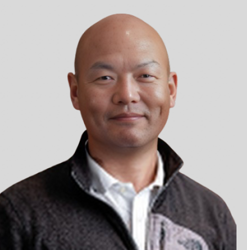
Pietro Scalia
Renesas Electronics
Company Profile
Renesas Electronics empowers a safer, smarter and more sustainable future where technology helps make our lives easier.
A leading global provider of microcontrollers, Renesas combines our expertise in embedded processing, analog, power and connectivity to deliver complete semiconductor solutions. These Winning Combinations accelerate time to market for automotive, industrial, infrastructure and IoT applications, enabling billions of connected, intelligent devices that enhance the way people work and live.

13:25 – 13:50
Challenges of Semiconductor Manufacturing – Design & Test Perspective in a Diversifying Market (Memory Case Study)
Shrinking modern Semiconductor Technologies and Geometries at the limit of Physics requires huge investments and economy of scales in multi billion dollar factories. Aside of inherent technical risks of operating at the limit of physics in sub 10nm technologies new challenges arose through geopolitical tensions as well as diversifying markets and applications. This presentation highlights such challenges. Future trends from a design & test perspective will be discussed how such risks could be managed and mitigated to achieve economically successful operation of such mega investments. Semiconductor Memory representing 30% of todays and future semiconductor sales will be used as a case study!

Marco Mezger
Neumonda
Marco Mezger is a global entrepreneur, investor, and advisor with over 25 years of experience in the semiconductor industry. Born in Germany and based in Taipei, Marco has a unique understanding of global semiconductor businesses with their challenges, resulting in a track record at various companies and as a matchmaker in the industry. As a thought leader focusing on memory technology, Marco has a sizeable global follower base on LinkedIn. He is also a regular guest on the business TV program “Taiwan Talks” commenting on the semiconductor industry news and market trends.
Company Profile
Neumonda has been founded with profound know how and the ‘DNA’ of former German memory powerhouse ‘Qimonda’. It has the ability to provide memory and storage solutions to worldwide customers, especially targeting the industrial and specialty market segments.
“Deep understanding of the technical/supply chain aspects of product design and developments, in addition to sales and marketing are building the foundation of the the global management team to serve these markets with real ‘Memory Competency‘.”

13:30 – 14:15
Panel Discussion:
Topic: Global Landscape and Chinese Practices in the Automotive Chip Industry — How Standardization Synergy Empowers a Globalized New Ecosystem for the Automotive Industry 车规级芯片产业的全球格局与中国实践 —— 标准化协同如何赋能汽车产业全球化新生态

Moderator
Joseph Chou
POMME TECHNOLOGIES., LTD
Company Profile
POMME was established in 2015 and is located in Hsinchu, Taiwan. It is engaged in high-end wafer test integration and design services for the semiconductor industry, focusing on providing you with the most efficient wafer parameter test solutions. Such as IC Design house, foundry, IDM, testing company, assembly and packaging company, etc., to simplify work for engineers in different departments (such as: technology research and development, quality and reliability assurance, failure analysis, manufacturing, etc.). POMME can help turn all the measurement and analysis under numerous test results into a simple job, speeding up product throughput throughout semiconductor production.
POMME is the solution partner of Keysight Technologies, a world-renowned instrument manufacturer. With more than 16 years of long-term cooperation experience, POMME has developed into the only and most reliable partner of customers among semiconductor industry test integration system providers, with the most professional The technical team, adhering to the spirit of quality first and customer satisfaction, grows together with customers and employees.
Since its establishment, it has served the semiconductor industry chain in the Asia-Pacific region, with more than 300 customers. We use experienced teamwork to run your test work quickly and efficiently. We can provide test solutions that meet your unique needs every time.
Company Products & Services
POMME possesses the leading wide-bandgap semiconductor automotive electronic components and module test solution technology, and has officially become the exclusive distributor of ipTEST LTD. in the UK. It can provide a full range of measurement solutions more efficiently to meet your needs.
main products:
Power semiconductor wafers, chips, components, and power module testing solutions.
Electrical test probe station (manual/semi-automatic/automatic), all electrical test probe station standard/custom configuration.
Electrical test system upgrade/maintenance/calibration/expansion (HP/Agilent/HP/Keysight/Keithley).
OST (Entrusted Measurement)/WBG/Low Current/Reliability/Burn-In.


Panelist
Wu Qiuli
CATARC


Panelist
Liu Yongshun
Chery


Panelist
Marcus Kneifel, Ph.D.
onsemi
Dr. Marcus Kneifel joined onsemi in February 2025 and currently serves as senior vice president of systems engineering, responsible for delivering cutting-edge systems and executing best-in-class engineering practices to expand and support our automotive, industrial, AI and new emerging technologies in adjacent growth markets.
Dr. Kneifel is a seasoned leader with deep industry knowledge and a proven track record, bringing valuable expertise into key target markets for the company.
Before joining onsemi, Marcus was the Chief Technology Officer and Board Member at Preh Group, and the General Manager of Portfolio Management 800V BEV Power Electronics, Electrified Powertrain Technology at ZF Friedrichshafen. Prior to that, he spent more than 20 years at Robert Bosch, moving through the ranks to ultimately be the General Manager of Engineering Customer Projects, Driver Assistance Systems.
He holds a master’s degree in electrical engineering from both the University of Applied Sciences Braunschweig and the University of Bremen, as well as a PhD. in Power Electronics from the University of Bremen.
Company Profile
onsemi (Nasdaq: ON) is driving disruptive innovations to help build a better future. With a focus on automotive and industrial end-markets, the company is accelerating change in megatrends such as vehicle electrification and safety, sustainable energy grids, industrial automation, and 5G and cloud infrastructure. With a highly differentiated and innovative product portfolio, onsemi creates intelligent power and sensing technologies that solve the world’s most complex challenges and leads the way in creating a safer, cleaner, and smarter world.


Panelist
Sanan Semiconductor
Yeh, Nientze, Ph.D. in Electrical Engineering from National Central University, Taiwan. He has long been engaged in the research and industry of compound semiconductor materials and devices, especially having 25 years of industrial R&D experience in the field of wide band-gap semiconductor materials and devices. Proficient in the design and industrial manufacturing of compound semiconductor devices. Has served as a researcher at the Telecommunication Laboratories of Chunghwa Telecom Co, Ltd. and the technical head of a listed company in Taiwan. The research results have obtained more than 30 patent authorizations in the United States, Japan, the Chinese and Taiwan, and published more than 70 international journal papers. He has also participated as the project or subject leader in several major projects and national key R&D programs.
Currently serves as the technical director of Hunan Sanan Semiconductor Co, Ltd., responsible for the R&D and mass production of compound semiconductor power electronic devices, and successfully built a production line of wide band-gap semiconductor power electronic devices from epitaxy to devices.
Company Profile
Sanan Semiconductor is a wholly-owned subsidiary of the listed company Sanan Optoelectronics. Sanan is committed to becoming a world-class R & D, manufacturing and service platform for wide bandgap semiconductors. Sanan Semiconductor extended Sanan Optoelectronics’ 20-year compound semiconductor industrialization experience to the field of power electronics, and became a full-chain integration platform focusing on the wide bandgap semiconductor industry and providing the most comprehensive products and services.
Company Products & Services
Sanan Semiconductor’s silicon carbide (SiC) power products include automotive and industrial SiC Schottky barrier diodes (SBD) and SiC MOSFETs which provide key components with higher power density and higher energy conversion efficiency for the electric vehicles and renewable energy markets. These can then be applied to high-reliability applications such as electric vehicle drivetrains, charging stations, and solar photovoltaic inverters. Sanan Semiconductor is a member of the JEDEC JC-70 Wide Band Gap Semiconductor Standards Committee, which collaborated with the industry to provide process technologies and products with improved reliability and quality. The company also has a portfolio of AEC-Q101 certified products.
13:30 – 13:50

Lode Lauwers
imec
Lode Lauwers is Senior Vice President Business Development and Strategy in IMEC, the nanoelectronics R&D Center in Leuven, Belgium. His current focus is to architect new global R&D collaborations and related business models, in line with semiconductor technology initiatives in various continents currently in conception. In that role he also guides imec’s Corporate Business Development strategies in nanoelectronics. Since he joined IMEC in 2005, he had various leading roles in IMEC’s technology business development and partner relation management. He has been driving over 2 decades the build-out, growth and business foundations of imec’s flagship core program with leading IC manufacturers, foundries, equipment and material suppliers and design and system houses. Earlier, he has been general manager of an ASIC design house, part of a US-based ASSP provider for the telecom industry, and scientific advisor for government funding in local and European cooperative networks in micro-electronics and telecommunications. He has a PhD in Electrical Engineering from KU Leuven.
Company Profile
Imec is a world-leading research and innovation center in nanoelectronics and digital technologies. Imec leverages its state-of-the-art R&D infrastructure and its team of more than 5,500 employees and top researchers, for R&D in advanced semiconductor and system scaling, silicon photonics, artificial intelligence, beyond 5G communications and sensing technologies, and in application domains such as health and life sciences, mobility, industry 4.0, agrofood, smart cities, sustainable energy, education, … Imec unites world-industry leaders across the semiconductor value chain, Flanders-based and international tech, pharma, medical and ICT companies, start-ups, and academia and knowledge centers. Imec is headquartered in Leuven (Belgium), and has research sites across Belgium, in the Netherlands and the USA, and representation in 3 continents. In 2021, imec’s revenue (P&L) totaled 732 million euro.
Further information on imec can be found at www.imec-int.com.

13:35 – 13:55
Advancements in Silicon Photonics Through Heterogeneous Integration
Heterogeneous Integration (HI) is critical to silicon photonics as new materials improve specifications. HI supports advances in , telecom, quantum computing, AI, AR/VR and biomedical sensors. X-FAB will act as an open foundry offering a modular integration architecture for lasers, modulators and photodetectors using its 200mm MEMS toolset.

Stefan Ernst, Ph.D.
X-FAB
Stefan studied physics in Dresden, Germany, and Edinburgh, UK. He obtained his PhD in the field of low-temperature solid state physics. Since joining X-FAB in 2011, he worked in various positions in technology development, engineering and program management. In his current role as Marketing Director, Stefan overlooks the global Business Development for MEMS and Microsystems Technologies at the X-FAB Foundry Group.
Company Profile
X-FAB is one of the world’s leading specialty foundry groups for analog/mixed-signal semiconductor technologies with a clear focus on automotive, industrial, and medical applications. As a pure-play foundry, X-FAB provides manufacturing and design support services to customers that design analog/mixed-signal integrated circuits (ICs) and other semiconductor devices for use in their own products or the products of their customers. Its customers worldwide benefit from the highest quality standards, manufacturing excellence and innovative solutions by using X-FAB’s modular CMOS and SOI processes in geometries ranging from 1.0 µm to 110 nm, and its special micro-electro-mechanical systems (MEMS) processes. X-FAB is also the first pure-play foundry to provide comprehensive processing technologies for the wide-bandgap materials silicon carbide (SiC) and gallium nitride (GaN). The GaN-on-Si wafers are manufactured in its modern 8” fab in Dresden, Germany, and SiC wafers in the 6” fab in Lubbock, Texas, USA. X-FAB runs six production facilities in Germany, France, Malaysia and the U.S. The company employs about 4,200 people worldwide.

13:35 – 13:55
Keynote

Hiroshi Iwatsubo
Murata Manufacturing Co., Ltd.
Hiroshi Iwatsubo graduated from Kyoto University, Department of Technology. He joined Murata Manufacturing Co., Ltd. in Kyoto, Japan in 1985. After engaging in the development of ceramic materials for four years, he was dispatched to Murata Europe GmbH in 1989 until his return to Murata Japan in 1993.
In 2012, he was appointed to Vice President, Head of Global Sales & Marketing
In 2015, he was appointed to Senior Executive Vice President (Board Member) Corporate Technology & Business Development Unit, In 2020, Senior Executive Vice President .
Hiroshi Iwatsubo currently serves as CTO and Executive Deputy President .

13:40 – 14:20
Panel Session: Evolving Trends for Advanced Packaging and the Challenges for Supply Chain and End User Applications

Moderator
Monita Pau, Ph.D.
Onto Innovation
Monita Pau is currently Strategic Marketing Director for Advanced Packaging at Onto Innovation. She works with business leaders and executives to drive strategic planning and leads the development of collaborative initiatives to drive growth and innovation. With over 15 years of experience, her expertise spans across frontend and backend of line process control solutions as well as specialty materials for advanced packaging and assembly. Prior to joining Onto, she held various positions in applications engineering, marketing and strategic business development at DuPont and KLA. Monita holds a Ph.D. degree in Chemistry from Stanford University.
Company Profile
Onto Innovation is a leader in process control, combining global scale with an expanded portfolio of leading-edge technologies that include: Un-patterned wafer quality; 3D metrology spanning chip features from nanometer scale transistors to large die interconnects; macro defect inspection of wafers and packages; elemental layer composition; overlay metrology; factory analytics; and lithography for advanced semiconductor packaging. Our breadth of offerings across the entire semiconductor value chain helps our customers solve their most difficult yield, device performance, quality, and reliability issues. Onto Innovation strives to optimize customers’ critical path of progress by making them smarter, faster and more efficient. Headquartered in Wilmington, Massachusetts, Onto Innovation supports customers with a worldwide sales and service organization.
General Telephone: +1 978 253 6200
General email: info@ontoinnovation.com
Website: www.ontoinnovation.com

Panelist
Vincent Kim, Ph.D.
Samsung Electronics
Dr. Vincent (WooPoung) Kim is the Corporate EVP, Head of Packaging at Samsung Device Solutions Research America based in San Jose, California. Dr. Kim is responsible for leading the packaging division at Samsung Device Solutions Research America, dedicated to meeting industry’s needs for advanced chip packaging in high-performance systems. Prior to joining Samsung, he served as a System Architect for Signal Integrity and Power Integrity at Apple, where he played a crucial role in developing consumer computers. Before his tenure at Apple, Dr. Kim worked as an SI Manager in Snapdragon packaging at Qualcomm. Prior to that, he was a Co-Design Engineer in the Wireless Business Unit of Texas Instruments, where he specialized in optimizing the electrical design of OMAP packages and systems. Dr. Kim also gained valuable experience as an SI Engineer at Rambus, where he designed and analyzed memory systems.
Dr. Kim received his Ph.D degree in Electrical and Computer Engineering (ECE) at Georgia Tech in 2004, and his M.S. & B.A. degrees from KAIST, Korea in 1999 and 1997.
Company Profile
Samsung Electronics Co., Ltd. engages in the manufacturing and selling of electronics and computer peripherals. The company operates through following business divisions: Consumer Electronics, Information Technology & Mobile Communications and Device Solutions. The Consumer Electronics business division provides cable television, monitor, printer, air-conditioners, refrigerators, washing machines and medical devices. The Information Technology & Mobile Communications business division offers handheld products, communication systems, computers and digital cameras. The Device Solutions business division comprises of memory, system large scale integrated circuit and foundry. The company was founded on January 13, 1969 and is headquartered in Suwon, South Korea.

Panelist
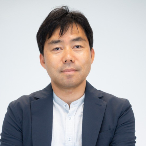
Jaesik Lee Ph.D.
SK Hynix
Dr. Jaesik Lee is Vice President of Package Engineering at SK hynix America. In this role, Jaesik is responsible for the research and development of advanced packaging for next generation High Bandwidth Memory (HBM) and pathfinding initiatives which enrich SK hynix’s innovations. He also focuses on the collaborations with customers to overcome HBM challenges associated with System in Packages (SIPs).
Prior to joining SK hynix America, Jaesik has held various key technical positions through Meta, Google, Nvidia, and Qualcomm where he drove advanced packaging technology developments, Packaging and System Co-optimization, and Manufacturing in Mobile, AI, and HPC applications. He received a PhD in mechanical engineering from University of Waterloo.
Company Profile
An AI First Mover Leading the Global AI Memory Era
With our global technology leadership, SK hynix aims to provide greater value to all stakeholders, including our customers, partner companies, investors, local communities, and employees.
Moreover, we are working to strengthen our ESG management to create even more value, by moving away from the conventional business model of seeking only economic benefits, in pursuit of more social value and a healthier governance structure.
SK hynix will grow into a Full Stack AI Memory Provider, offering customized solutions tailored to the diverse needs of global customers, covering both DRAM and NAND flash, in the era of full-scale AI.

Panelist
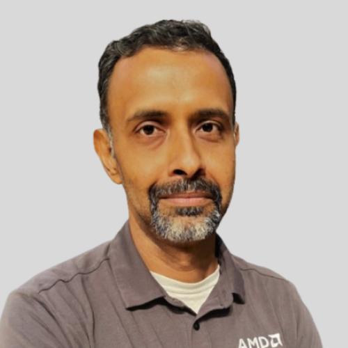
Raja Swaminathan, Ph.D.
AMD
Dr. Raja Swaminathan is the Corporate Vice President of Packaging at AMD, spearheading the development of AMD’s advanced packaging and heterogeneous integration roadmap. With a distinguished career spanning roles at Intel, Apple, and now AMD, Dr. Swaminathan’s expertise in design-technology co-optimization and dedication to optimizing power, performance, area, and cost (PPAC) have led to significant technological advancements such as EMIB, Apple’s Mx packages, 3D V-Cache, and 3.5D architectures for AI accelerators. Dr. Swaminathan holds a PhD from Carnegie Mellon University and an undergraduate degree from IIT Madras. With over 100 patents and more than 40 published papers to their name, Dr. Swaminathan was recently recognized as an IEEE Fellow and serves as a technical advisor to multiple startups. His unwavering commitment to heterogeneous integration continues to drive the boundaries of silicon technology.
Company Profile
For 50 years, AMD has driven in high-performance computing, graphics, and visualization technologies – the building blocks for gaming, immersive platforms, and the datacenter. Hundreds of millions of consumers, leading Fortune 500 businesses and cutting-edge scientific research facilities around the world rely on AMD technology daily to improve how they live, work and play. AMD employees around the world are focused on building great products that push the boundaries of what is possible. For more information about how AMD is enabling today and inspiring tomorrow, visit AMD (NASDAQ:AMD) on their website, blog, Facebook and Twitter pages.


Panelist
SkyWater Technology
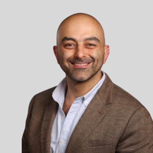
Bassel Haddad is Sr Vice President and General Manager of Advanced Packaging at SkyWater Technology. He leads all aspects of SkyWater’s advanced packaging business including technology development, engineering, marketing and Florida fab operations. He is responsible for building and scaling the business serving both the defense and commercial market sectors. He is focused on strengthening collaborations with the advanced packaging ecosystem, such as equipment and material vendors, government partners and research institutes & consortia, while driving the growth trajectory of the business.
Before joining SkyWater, Haddad was with Intel since 2011 holding various engineering and business leadership roles. Most recently, he was the Vice President and General Manager of edge device and AI products, in the network and edge group. In this role, he managed a multi-billion dollar P&L, and leading innovations in edge AI and Internet of Things, or IoT. Earlier in his career, he held roles in platform architecture, silicon development, systems and software engineering, delivering leadership products to various end markets.
Haddad holds a Bachelor’s and Master’s degree in electrical engineering from Technion – Israel Institute of Technology. He is the inventor of five USPTO-issued patents in the areas of digital communication and systems architecture.
Company Profile
SkyWater (NASDAQ: SKYT) is a U.S.-based semiconductor manufacturer and a DMEA-accredited Category 1A Trusted Supplier. SkyWater’s Technology as a Service model streamlines the path to production for customers with development services, volume production and heterogeneous integration solutions in its U.S. facilities. This pioneering model enables innovators to co-create the next wave of technology within diverse categories including mixed-signal CMOS, ROICs, rad-hard ICs, MEMS, superconducting ICs, photonics and advanced packaging. SkyWater serves the growing markets of aerospace & defense, automotive, biomedical, industrial and quantum computing. For more information, visit: www.skywatertechnology.com.

13:40 – 14:05
CASE STUDY (Cost): Cutting Costs Without Compromise
Reserved
13:45 – 13:55
Disruption in Semiconductor Industry
For over 40 years, AlixPartners has been helping clients confront disruption. Increasingly, cycles of disruption have displaced economic cycles as the primary business challenge.
Disruption is the new economic driver. We will share the results our 6th annual AlixPartners Disruption Index, with particular insights on how CEOs and senior executives of the semiconductor industry perceive major disruptions, opportunities and challenges in this exciting field around the globe.

Janet Tang
AlixPartners
Janet brings 20 years of a variety of industry experience such as as chief strategy officer (CSO) of a Global 500 company, oversight of P&L responsibilities, service in consulting leadership, role as a software architect, and engagements in entrepreneurship. Janet is known for successfully driving complex transformations in technology firms and telcos, turning around cost centers into profit centers, building transformative go-to-market engines, and coaching next generations of client leaders. Her early career as a software architect in Silicon Valley also gave her hands-on experience in R&D and product management.
Janet has a Master of Science in Computer Science from Stanford University. She has served as a board member of the University of Toronto Engineering Alumni Network and as chair of the network’s Nomination and Governance Committee.
Company Profile
AlixPartners is a results-driven global consulting firm that specializes in helping businesses respond quickly and decisively to their most critical challenges—from urgent performance improvement to complex restructuring, from risk mitigation to accelerated transformation. These are the moments when everything is on the line—a sudden shift in the market, an unexpected performance decline, a time-sensitive deal, a fork-in-the-road decision. We stand shoulder to shoulder with our clients until the job is done, and only measure our success in terms of the results we deliver.
Company Products & Services
Clients call us when they need pragmatism and cut-through to solve their most complex challenges arising from a continually disrupted world. Our services cover Artificial Intelligence, Corporate Strategy & Transformation, Data Governance, ESG, Growth, Investigations, Disputes & Advisory Services, Mergers & Acquisitions, Organizational Transformation, Supply-Chain Management & Operations, Technology, Transformative Leadership and Turnaround and Restructuring.

13:45 – 14:05
Reserved speak slot for Embeded Chip Packaging topic / Hyundai Mobis

Avinash Kashyap Ph.D.
Vishay Intertechnology, Inc.
Dr. Avinash Kashyap is the Senior Vice President & Division Head of the MOSFETs Division at Vishay Intertechnology. He leads a global organization overseeing P&L, engineering, marketing, applications, and revenue generation for power products, including Si MOSFETs, Power ICs, and SiC, with a strong focus on automotive, industrial, and data center applications.
Previously, Dr. Kashyap served as Vice President & General Manager of the Discrete & Wide Bandgap Power Business Unit at Renesas Electronics, where he led multiple product lines, including IGBTs, SiC, Si MOSFETs, and GaN, catering to high-volume markets.
Throughout his career, Dr. Kashyap has held leadership roles at Microchip Technology and GE Global Research, where he played a pivotal role in advancing wide bandgap technologies and successfully bringing them to market.
An accomplished innovator, he has authored over 35 peer-reviewed publications and holds more than 20 patents (granted or pending). Dr. Kashyap earned his M.S. and Ph.D. in Electrical Engineering from the University of Arkansas, Fayetteville. He is a Senior Member of IEEE and a distinguished member of the Arkansas Academy of Electrical Engineers.
Company Profile
Vishay Intertechnology, Inc., a Fortune 1000 Company listed on the NYSE (VSH), is one of the world’s largest manufacturers of discrete semiconductors (diodes, rectifiers, MOSFETs, optoelectronics, and selected ICs) and passive electronic components (resistors, inductors, and capacitors). These components are used in virtually all types of electronic devices and equipment, in the industrial, computing, automotive, consumer, telecommunications, military, aerospace, power supplies, and medical markets. Vishay’s product innovations, successful acquisition strategy, and “one-stop shop” service have made it a global industry leader.

13:50 – 14:10
Reserved for Micron Technology
13:50 – 14:10

Giorgia Longobardi, Ph.D.
Cambridge GaN Devices
Dr. Giorgia Longobardi, CEO of CGD, is an experienced engineer with international practice working on GaN power devices design and characterisation. As the inventor of high impact patents in the field of GaN power devices, Giorgia made the unique blend of academic and business know-how one of her biggest strengths.
During her PhD in power devices at Cambridge University, Giorgia worked on international projects with top semiconductor companies, through which, she learned about different cultures operating in this field and gained experience managing and budgeting multi-partner projects. Curious and knowledgeable, Giorgia leads an experienced diverse team of passionate people working with enthusiasm and continuous drive to do things better. She never forgets why she founded CGD: to change how energy is used and protect the environment with efficient power electronics.
She is a member of the energy management committee at PSMA (power Sources manufacturers association) and Strategic Advisory Board at the Henry Royce Institute for materials.
Company Profile
A spin-out of the Cambridge University, Cambridge GaN Devices (CGD) is a fabless semiconductor company that develops a range of energy-efficient GaN-based power devices to make greener electronics possible.
Operating at a market worth exceeding $30 billion, CGD completed several funding rounds to develop and deliver to the market a wide range of products for consumer and industrial applications.
In autumn 2021, the company was named Tech Scaleup of the Year by Business Weekly in the category of green electronics and was awarded the UK Business Angels Association (UKBAA) deep tech Investment of the Year.

13:50 – 14:15
Alternative Career Paths Help the Semiconductor Industry Meet Workforce Needs
We’re facing an unprecedented demand for resources within our industry. Our existing workforce is retiring, we’re building more manufacturing capacity than ever before and together with the impact caused by the pandemic we find ourselves with a challenge that is undoubtedly going to be the number one issue in the coming years and that is talent. With experienced individuals leaving the workforce and not enough new people joining, the talent pipeline is not meeting current demand. In this session, we will discuss these challenges and how a more collaborative partnership model might be the right approach for businesses looking to fill staff vacancies and for individuals looking to start their careers in this exciting industry.

Geoffrey Stoddart
WGNSTAR
Company Profile
WGNSTAR, formerly Westerwood Global and NSTAR Global Services, and as of June ’24 WGNSTAR acquired Principle Service Solutions (PSS), provide innovative and cost-efficient managed workforce services and asset lifecycle management solutions. We partner with our clients to:
With regional offices throughout the United States and Ireland, we are strategically located where our clients need us most. Visit us at: www.wgnstar.com

Romain Fraux
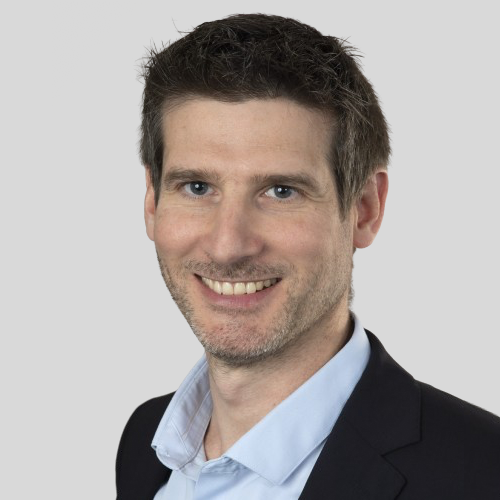
Yole Group
Romain Fraux serves as the Chief Research Officer at Yole Group, leveraging his extensive expertise in the semiconductor industry to lead the development of the organization’s global operations.
He oversees a team of analysts dedicated to exploring the semiconductor landscape, encompassing “More Moore” and “More than Moore” technologies, semiconductor manufacturing, and the global supply chain, with the goal of identifying innovations and business opportunities.
Under Romain’s leadership, Yole Group’s international team delivers comprehensive services, including market research, technology and strategy analysis, reverse engineering and cost assessment, and module performance evaluation. These insights empower Yole Group’s clients to make informed decisions about their future business and manufacturing strategies in the semiconductor, photonics, and electronics sectors.
In his cross-functional executive role, Romain represents Yole Group during key client engagements and regularly shares the organization’s strategic vision at leading international conferences. With over 15 years at Yole Group, he has been instrumental in shaping its position as a thought leader in the industry.
Romain holds a bachelor’s degree in Electrical Engineering from Heriot-Watt University in Edinburgh (Scotland), a master’s degree in Microelectronics from the University of Nantes (France), and an MBA (IEMN – IAE, France).
Company Profile
Yole Group is a leading international market research and strategy consulting firm, delivering in-depth analyses across market trends, technology developments, teardowns, and reverse costing. Leveraging deep semiconductor expertise, its team of analysts also provides custom consulting services, offering strategic, technical, and market insights tailored to address specific business challenges and opportunities.

13:55 – 14:15
Daisuke Murata
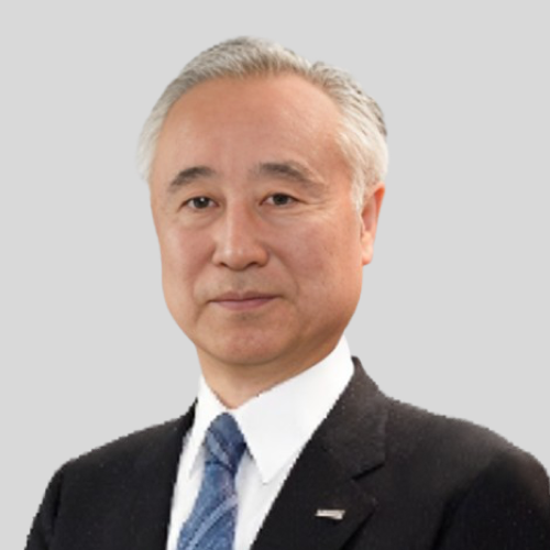
Murata Machinery
Daisuke Murata has served as President and CEO of Murata Machinery, since September 2003. He has held a variety of ascending leadership positions at Murata Machinery since 1987.
He also now serves as Chairman of the Japan Textile Machinery Association, as Chairman of the Japan Institute of Material Handling, and Superintendent of the Japan Business Machine and Information System Industries Association. In July 2017, he became the SEMI International Board member.
He graduated with a Bachelor of Economics from Hitotsubashi University in 1984 and obtained MBA from the Graduate School of Business at Stanford University in 1990.
Company Profile
Murata Machinery (Muratec) is a worldwide leader and solution provider for automated material handling systems in semiconductor manufacturing and other manufacturing or distribution industries. Muratec also manufactures machinery and equipment such as Textile Machinery, Machine Tools, Sheet Metal Machinery, and Communication Equipment.
This year marks 90 years since its founding in 1935. Under the slogan “Innovation. Mark the turning point”, Muratec aims to create technologies that bring innovation to the market and society.
Company Products & Services

13:55 – 14:15
From Sensing to Thinking: The Evolution of MEMS with Embedded AI
2024 was a welcome turning point for the MEMS industry, with global revenue estimated at $15.4 billion. This is primarily due to the winding down of the inventory stockpiling in the second quarter of 2024. The race for innovation is crucial to maintaining a high sensor value and stabilizing the average selling price (ASP). Implementing first-stage data processing at the sensor level is one possible solution that brings several advantages, from power consumption to versatile applications and ease of integration.
The presentation will provide an overview of the current status of the MEMS industry, key trends expected over the next five years, and insights into the evolution of the MEMS ecosystem within the global economic context.

Pierre-Marie Visse
Yole Group
Pierre-Marie Visse is Senior Technology & Market Analyst, MEMS & Sensing at Yole Group. He is working within the Photonics & Sensing team. Pierre-Marie contributes daily to the technical, marketing, and strategic analysis on various MEMS and sensing technologies.Prior to Yole Group, Pierre-Marie served as an R&D project manager at eLichens, specializing in the detection of environmental gases, for more than 2 years. His primary focus was the development of gas sensors and IoT for gas detection. Previously, Pierre-Marie worked at TDK-Tronics for more than ten years as an inertial MEMS designer for custom sensors, accelerometers, and gyroscopes. He then worked as an R&D project manager for the navigation, industrial, and watchmaking industries. Pierre-Marie graduated from ESIEE-Engineering (France) in 2010, specializing in microsystems.
Company Profile
Yole Group is a leading international market research and strategy consulting firm, delivering in-depth analyses across market trends, technology developments, teardowns, and reverse costing. Leveraging deep semiconductor expertise, its team of analysts also provides custom consulting services, offering strategic, technical, and market insights tailored to address specific business challenges and opportunities.

14:00 – 18:00
Registration
14:00 – 14:10
The Future of Atomic Layer Advanced Manufacturing
ATLANT 3D is pioneering a new era of atomic-scale manufacturing, enabling the creation of materials and devices with unprecedented precision. Our patented Direct Atomic Layer Processing (DALP®) technology redefines microfabrication, bridging the gap from lab to fab. With our NANOFABRICATOR™ platform, research teams and industries can develop next-generation quantum, semiconductor, advanced packaging, MEMS/sensors and space technologies faster and more efficiently. By replacing complex, resource-intensive processes with precise atomic-scale fabrication, we empower innovators to build the technologies of tomorrow while driving sustainability. Join us to explore how atomic control is unlocking new possibilities for advanced manufacturing and scientific breakthroughs.

Bonnie Tsim, Ph.D.
ATLANT 3D
Dr. Bonnie Tsim is Head of Strategic Initiatives at ATLANT 3D and holds a PhD in Theoretical Physics on the electronic properties of twistronic graphene from the University of Manchester. With expertise across deep-tech strategy, advanced materials, and international ecosystem building, she has led AI strategy and digital transformation at Turner & Townsend and convened global stakeholders in exponential technologies such as quantum and semiconductors at MATTER.
Company Profile
ATLANT 3D has mastered control of matter at the atomic scale, ushering in a new era in manufacturing. For research teams and manufacturers working at the frontiers of technology, we’ve created what was once thought unattainable: a system that builds materials and devices, atom by atom, with unprecedented precision and speed.
While others are constrained by traditional manufacturing limits, our breakthrough technology makes it possible to create the seemingly impossible, from next-generation quantum computers to devices that can operate in the harsh conditions of space. By replacing complex, resource-heavy processes with precise atomic-scale fabrication, we’re transforming technology while making manufacturing sustainable. We’re providing innovative teams the power to build technologies today that will define tomorrow’s world, using fewer resources to achieve greater possibilities.
Based in Copenhagen and London, with operations in the US, ATLANT 3D partners with research institutions and industrial companies to expand the boundaries of technological possibility.
Company Products & Services
ATLANT 3D is redefining microfabrication with its patented Direct Atomic Layer Processing (DALP®) technology. Our NANOFABRICATOR™ platform enables localized atomic layer processing for rapid material discovery, prototyping, and scalable device fabrication—bridging the gap from lab to fab.
Beyond hardware, we offer Pilot Projects and Joint Development Services to validate new materials and device architectures. A-HUB, our Microfabrication-as-a-Service (MaaS) centre, provides R&D teams with atomic-scale precision without the need for costly infrastructure.
From concept to fabrication, ATLANT 3D partners with academia and industry to drive next-generation innovations beyond conventional limits.

Day 1 Afternoon Session Moderator
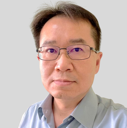
Yu-Hua Chen, Ph.D.
Unimicron Technology Corp
Education:
Experience:
Company Profile
Founded in 1990, Unimicron is a world leading company of printed circuit board (PCB) and IC carrier (substrate) manufacturing. Major products include PCBs, high density interconnection (HDI) boards, flexible PCBs, rigid flex PCBs, and IC substrates. Product applications include AI, HPC data center infrastructure (server, networking), smartphones, PC/NB, optical modules, automotive and more. Unimicron’s global footprint encompass manufacturing sites and/or service centers in Taiwan, China, Germany, Japan and Thailand, delivering high value-added, high quality and high productivity innovation and services to our global customers.
Company Products & Services
Unimicron’s high-end substrate solutions, FCBGA and FCCSP, provide our valued customers the technologies crucial in meeting today’s fast-growing development of AI, HPC applications. Our customer-oriented service, high quality standards, and innovative breakthroughs have helped Unimicron achieve the honor of No.1 ranking among the global substrate suppliers by market share for the 9th consecutive year since Y2016.

14:05 – 14:15
Disruption of the semiconductor industry
Based on AlixPartners’ Disruption Index survey of over 3,000 executives globally, several striking trends emerged that show how the semiconductor industry’s resilience is being tested amid geopolitical pressures and the transformative impact of AI. I will discuss the industry leaders’ outlook into the future, how market leaders are navigating geopolitical tensions, tariffs, and supply chain disruptions as well as implementing AI role in driving growth and evolving workforce needs. The survey shows that forward-looking leaders are optimistic about AI’s potential to enhance revenues and manufacturing capabilities and proactively change business and operating models to be the drivers of disruptions.

Markus Bolte, Ph.D.
AlixPartners
Markus co-leads AlixPartners’ global semiconductor practice. With 20 years of global business experience, he serves clients on their business and operating model transformation and change journeys. He is driven by a passion for measurable impact and the desire to help the semiconductors industry navigate through the disruptions of our age. Before joining Alixpartners, Markus led the strategy at a global technology leader. He started his consulting career at two leading European management consultancy firms. Before joining the consulting world, Markus led a research group for supercomputing and nanophysics research utilizing Nvidia’s CUDA to accelerate complex nanophysics simulations and collaborating with institutions globally. Markus holds a PhD and Masters in Physics and Computer Science.
Company Profile
AlixPartners is a results-driven global consulting firm that specializes in helping businesses respond quickly and decisively to their most critical challenges—from urgent performance improvement to complex restructuring, from risk mitigation to accelerated transformation. These are the moments when everything is on the line—a sudden shift in the market, an unexpected performance decline, a time-sensitive deal, a fork-in-the-road decision. We stand shoulder to shoulder with our clients until the job is done, and only measure our success in terms of the results we deliver.
Company Products & Services
Clients call us when they need pragmatism and cut-through to solve their most complex challenges arising from a continually disrupted world. Our services cover Artificial Intelligence, Corporate Strategy & Transformation, Data Governance, ESG, Growth, Investigations, Disputes & Advisory Services, Mergers & Acquisitions, Organizational Transformation, Supply-Chain Management & Operations, Technology, Transformative Leadership and Turnaround and Restructuring.

14:05 – 14:50

Moderator
Hamid Azimi, Ph.D.
International Semiconductor Industry Group (I.S.I.G.)
Dr Hamid Azimi, formerly Corporate VP, Director of Substrate Packaging TD of Intel. He was responsible for advanced substrate packaging for all Intel logic products across substrate suppliers’ factories, as well as the company’s two internal substrate R&D factories. These R&D factories are the birthplace of panel level die embedding technology and play a crucial role for enabling EMIB, the key technology to Intel’s data-centric business and heterogenous packaging. His team works with equipment, material, chemical and substrate suppliers to develop Si-fab backend-like technologies for panel level advanced packaging, and transfer technologies to Intel supplier factories to meet the demand of future Intel products.
Company Profile
Established in 2010, the International Semiconductor Industry Group (ISIG) is a prestigious and trusted global platform, known for fostering collaboration and driving innovation across the semiconductor industry. With a strong foundation through its International Semiconductor Executive Summits (I.S.E.S.), ISIG orchestrates influential regional summits across the U.S., Middle East, Europe and Asia, fully endorsed by local governments and leading companies throughout the semiconductor supply chain.
At ISIG, we are more than just event organizers—we serve as a catalyst for shaping the future of the semiconductor industry. Through high-level executive recruitment, expert consultation, and strategic investor engagement, ISIG empowers global collaboration, helping industry leaders connect, collaborate, and innovate. Our vision is to create a trusted network that transcends borders and disciplines, uniting government officials, academic experts, and investors to tackle the most pressing challenges and seize the greatest opportunities in the semiconductor ecosystem.
Together, we ensure the semiconductor industry remains at the forefront of technological advancement and economic growth, shaping a sustainable future for the global market.


Panelist
Raja Swaminathan, Ph.D.
AMD
Dr. Raja Swaminathan is the Corporate Vice President of Packaging at AMD, spearheading the development of AMD’s advanced packaging and heterogeneous integration roadmap. With a distinguished career spanning roles at Intel, Apple, and now AMD, Dr. Swaminathan’s expertise in design-technology co-optimization and dedication to optimizing power, performance, area, and cost (PPAC) have led to significant technological advancements such as EMIB, Apple’s Mx packages, 3D V-Cache, and 3.5D architectures for AI accelerators. Dr. Swaminathan holds a PhD from Carnegie Mellon University and an undergraduate degree from IIT Madras. With over 100 patents and more than 40 published papers to their name, Dr. Swaminathan was recently recognized as an IEEE Fellow and serves as a technical advisor to multiple startups. His unwavering commitment to heterogeneous integration continues to drive the boundaries of silicon technology.
Company Profile
For 50 years, AMD has driven in high-performance computing, graphics, and visualization technologies – the building blocks for gaming, immersive platforms, and the datacenter. Hundreds of millions of consumers, leading Fortune 500 businesses and cutting-edge scientific research facilities around the world rely on AMD technology daily to improve how they live, work and play. AMD employees around the world are focused on building great products that push the boundaries of what is possible. For more information about how AMD is enabling today and inspiring tomorrow, visit AMD (NASDAQ:AMD) on their website, blog, Facebook and Twitter pages.

Panelist
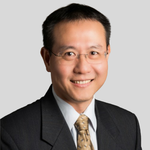
Jim Li, Ph.D.
ASE
Company Profile
ASE is the leading global provider of semiconductor manufacturing services in assembly and test. With a proven track record spanning almost 40 years, ASE today is at the forefront of flexible, powerful, integration technologies that achieve criteria for improved power, performance, area, and cost requirements. Our comprehensive toolbox leveraging innovative technologies, such as die interconnection, wafer level fan out, embedded devices, conformal and compartmental shielding, integrated antenna, and others, are being refined and enhanced to support future generations of system integration. Heterogenous Integration through SiP is enabling significant innovation across dynamic application areas including AI, 5G, automotive, mobile, IoT and more. Our industry is driven by innovation, and through ASE’s miniaturization technologies, we are enabling transformative solutions that are literally changing lives, from health to transportation, from Robotics to AI, from IoT to 5G.
Website: ase.aseglobal.com

Panelist
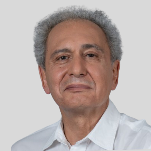
Babak Sabi, Ph.D.
AWS Annapurna Labs
Dr. Babak Sabi is VP of Technology at AWS/Annapurna Lab. Babak joined AWS in 2024 after 40 years in Intel. Babak was Senior Vice President and the General Manager of Assembly & Test Technology Development (ATTD) at Intel Corporation. Since 2009, he has been responsible for the company’s packaging, assembly, and test process technology development. During Babak’s tenure in ATTD 2.5D and 3D Advanced Packages were developed and ramp to high Volume Manufacturing. Additionally ATTD team made many advancement in Substrate and Test Technology.
Prior to leading ATTD, Babak oversaw Intel’s Corporate Quality Network from 2002 to 2009 where he led product reliability, customer satisfaction and quality business practices.
Babak joined Intel in 1984 after receiving Babak his Ph.D. in solid state electronics from Ohio State University in 1984.
Company Profile
Launched in 2006, Amazon Web Services (AWS) began exposing key infrastructure services to businesses in the form of web services — now widely known as cloud computing. The ultimate benefit of cloud computing, and AWS, is the ability to leverage a new business model and turn capital infrastructure expenses into variable costs. Businesses no longer need to plan and procure servers and other IT resources weeks or months in advance. Using AWS, businesses can take advantage of Amazon’s expertise and economies of scale to access resources when their business needs them, delivering results faster and at a lower cost.
Today, Amazon Web Services provides a highly reliable, scalable, low-cost infrastructure platform in the cloud that powers hundreds of thousands of businesses in 190 countries around the world. With data center locations in the U.S., Europe, Singapore, and Japan, customers across all industries are taking advantage of our low cost, elastic, open and flexible, secure platform.


Panelist
Onto Innovation
Mike Rosa is chief marketing officer (CMO) and senior vice president responsible for strategy at Onto Innovation. Prior to his current role, Mike served as CMO for Applied Materials ICAPS and Advanced Packaging Groups, where he was responsible for leadership of strategic and technical marketing, marketing communications, charting device segment inflection roadmaps and providing strategic business development support toward M&A activities. He has over 25 years’ experience in semiconductor engineering and technology, with roles that span device design and fabrication, equipment development, marketing and sales. His technical qualifications include B.Eng. (Hons) and Ph.D. degrees in Microelectronic Engineering and an MBA with dual majors in Marketing and Business Strategy. Mike has authored over 40 journal and conference publications and holds over 29 U.S. patents
Company Profile
Onto Innovation is a leader in process control, combining global scale with an expanded portfolio of leading-edge technologies that include: Un-patterned wafer quality; 3D metrology spanning chip features from nanometer scale transistors to large die interconnects; macro defect inspection of wafers and packages; elemental layer composition; overlay metrology; factory analytics; and lithography for advanced semiconductor packaging. Our breadth of offerings across the entire semiconductor value chain helps our customers solve their most difficult yield, device performance, quality, and reliability issues. Onto Innovation strives to optimize customers’ critical path of progress by making them smarter, faster and more efficient. Headquartered in Wilmington, Massachusetts, Onto Innovation supports customers with a worldwide sales and service organization.
General Telephone: +1 978 253 6200
General email: info@ontoinnovation.com
Website: www.ontoinnovation.com

Panelist
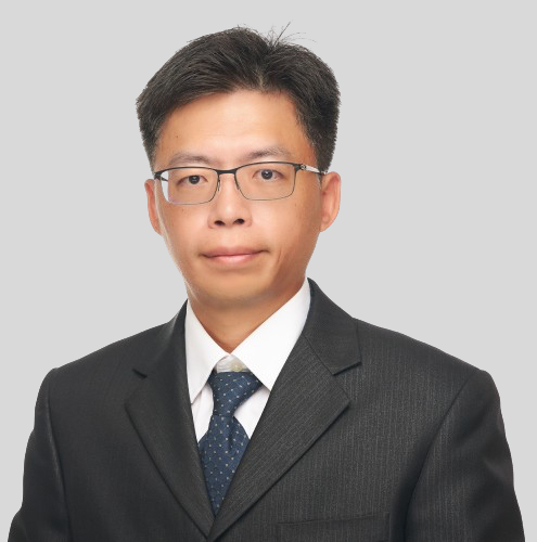
Jim Lin, Ph.D.
Powertech Technology Inc.
Dr. Jim Lin is Vice President of Advanced Technology & Wafer Level Package Operation. He is in charged of advanced packaging R&D, Business and Operation in PTI. Prior to BU head, Dr. Lin was AVP of Memory Packaging Research & Development. Dr. Lin joined PTI in 2006, led the development of memory packaging technology. Developed technologies including 8 to 32 chips memory stacking package, system integrated package of SSD, Package on Package(PoP), Heterogeneous multi-chip package(MCP), 3D TSV interconnection High Bandwidth Memory(HBM) and Fan-out Panel Level Package (FOPLP). Dr. Lin received his M.S. and Ph.D. degree both from National Tsing Hua University in Power Mechanical Engineering.
Company Profile
Powertech Technology Inc. (PTI), the world’s leading OSAT, was founded in 1997. We serve the international customers with services including chip bumping, chip probing, IC assembly, final testing, burn in, and system level assembly. In 2017 PTI expanded the production base to Japan to serve the local automotive electronics and IoT market. And in 2018, PTI began the construction of the newest Fan Out Panel Level Package manufacturing facility in Hsinchu Science Park.
PTI has over 18,000 employees world wide, and manufacturing facility located in Taiwan, China and Japan. PTI dedicates her efforts in developing advanced technologies, while carrying on as the world’s leading memory packaging and testing solution provider. Through strategic alliances and resource integration, PTI group relentlessly marches onward in the semiconductor packaging and testing field.
We drive our future growth with outstanding quality, cost, and delivery. Promise, Technology, and Integration represents our core values. With our ideaology, strategy, and core values, PTI stands as the world class OSAT.
Company Products & Services
PTI offers the services inculding Final test, Chip Probe, IC Packaging, Module Assembly, Quality Management. And provide wide range of technology solution for IC packaing including Panel Level Fan Out, TSV solution, Bumping, Flip chip, Antenna in Package.
-Panel Level Fan Out
Fan-out packaging is going to become the mainstream for high-end device application, especially for multi-die, heterogeneous integration for both active & passive devices. High density interconnect, excellent performance in electrical performance and power consumption can also be achieved by panel FO. PTI’ Panel level FO packaging offers the merits of high production efficiency with better utilization & unit output in comparison to wafer level FO.
Solution: CHIEFS® / CLIP® / PiFO® / BF2O®
TSV Solution-3DIC
3D IC is one kind of heterogeneous technology which is integrated vertically by Si wafers or chips. The interconnection is composed by u-bumps and Through Silicon Via (TSV). TSV fabrication is regarded as the heart of 3D IC because it provides the advantages of shortening the interconnection path, high function density, low power consumption, smaller form factor and high performance; these benefits make 3D IC get commercial success in some specific applications, such like HPC and AI.
TSV Solution-CMOS Image Sensor
CMOS Image Sensor (CIS) is an electronic device that converts an optical image into an analog signal. Recently, the most attractive is stack-CIS, that BSI CIS, memory wafer and Image Signal Processor(ISP) wafer are vertically integrated and higher performance, lower power consumption would be the advantages for high-end application.
Bumping
Wafer bumping is a metal bump that grows on a wafer, and each bump is an IC signal contact. Unlike conventional interconnection through wire-bond, bond pads are placed at peripheral area , IO pads for bumping could be distributed all over the surface of the chip, thus chip size could be shrunk and electrical path could be optimized.
14:10 – 14:30
Reserved for Samsung
14:10 – 14:30

Taylor Li
JCET
Company Profile
JCET Group is the world’s leading integrated-circuit manufacturing and technology services provider, offering a full range of turnkey services that include semiconductor package integration design and characterization, R&D, wafer probe, wafer bumping, package assembly, final test and drop shipment to vendors around the world.
Our comprehensive portfolio covers a wide spectrum of semiconductor applications such as mobile, communication, compute, consumer, automotive, and industrial, through advanced wafer-level packaging, 2.5D/3D, System-in-Package, and reliable flip chip and wire bonding technologies. JCET Group has two R&D centers in China and Korea, six manufacturing locations in China, Korea, and Singapore, and sales centers around the world, providing close technology collaboration and efficient supply-chain manufacturing to our global customers.

14:10 – 14:55
PANEL (Cost): Sustainability & Sustainable Cost Control

Panelist
Henri Berthe
Schneider Electric
Henri Berthe, a seasoned professional with 20 years of experience at Schneider Electric, leads the global Semiconductor Segment, driving sustainability and digitization. Previously, he was VP of Universal Enclosures, overseeing a global business focused on high-quality, standard, and connected enclosures. Before that, he served as VP of Digital Energy in MENA and Africa, deploying digital technologies and electrification solutions. Henri’s expertise spans energy management, digital power, and building management systems. He holds a master’s degree in Sales and Marketing from ESTA Belfort, France. In May 2024, he joined the Regional Advisory Board of SEMI South-East Asia and the Global Counsel of the Semiconductor Climate Consortium.
Company Profile
Schneider Electric is the global industrial technology leader, driving sustainable impact.
We are a powerhouse of electrification, automation, and digitization. The unique combination of our electrical and automation technologies intersect with our leadership in software, services and sustainability to rapidly accelerate sustainable impact.
Schneider’s purpose is to create Impact by empowering all to make the most of our energy and resources, bridging progress and sustainability for all. At Schneider we call this Life Is On.
Our mission is to be the trusted partner in Sustainability and Efficiency.
Company Products & Services
Energy management, Industrial Automation, Sustainability and Consulting Services, Industrial Software.


Panelist
Reserved
STMicroelectronics
Company Profile
At ST, we are more than 50,000 creators and makers of semiconductor technologies mastering the semiconductor supply chain with state-of-the-art manufacturing facilities. An integrated device manufacturer, we work with more than 200,000 customers and thousands of partners to design and build products, solutions, and ecosystems that address their challenges and opportunities, and the need to support a more sustainable world. Our technologies enable smarter mobility, more efficient power and energy management, and the wide-scale deployment of cloud-connected autonomous things. We are committed to achieving our goal to become carbon neutral on scope 1 and 2 and partially scope 3 by 2027. Further information can be found at www.st.com.


Panelist
Skyworks Solutions
Company Profile
Skyworks Solutions, Inc. is empowering the wireless networking revolution. Our highly innovative analog semiconductors are connecting people, places and things spanning a number of new and previously unimagined applications within the automotive, broadband, cellular infrastructure, connected home, industrial, medical, military, smartphone, tablet and wearable markets.
Skyworks is a global company with engineering, marketing, operations, sales and support facilities located throughout Asia, Europe and North America.
Company Products & Services
Skyworks products are used in aerospace, automotive, broadband, cellular infrastructure, connected home, defense, entertainment and gaming, industrial, medical, military, smartphone, tablet, and wearable markets.

14:15 – 14:20
I.S.I.G. Closing Remarks
14:15 – 14:35
How foundry services can help to build customized solutions in an evolving SiC Market?
In the rapidly advancing field of renewable energy, Silicon Carbide (SiC) technology stands as a key enabler of the next generation of high-performance power electronics. Here we will examine the critical challenges and emerging opportunities within the sector and highlight how X-FAB innovations are providing a powerful platform for the accelerated development and deployment of customized SiC solutions.
The growing adoption of EV applications, the power bottleneck in data centers and the need for renewable energy solutions has compelled X-FAB to focus it efforts on creating high performing products for automotive, industrial and energy markets, We leverage our expertise in SiC technology and our advanced approach to process integration, we have optimized development cycles, dramatically reducing time to market and equipping customers with a distinct competitive advantage. Attendees will gain valuable insights into how our comprehensive solutions drive rapid innovation, accommodate diverse customer needs, and support the scalable adoption of SiC technologies in propelling global renewable energy initiatives forward.

Rico Tillner
X-FAB
Rico Tillner has 19 years of experience in the semiconductor industry. After his master’s degree in electrical engineering at Technical University Dresden he started his career at X-FAB Dresden. From 2007 until 2015 he worked as Process integration engineer, responsible for a 0.6µm automotive mixed signal technology. In 2016 he becomes the quality manager of X-Fab Dresden. From 2018 until 2023 Rico Tillner was the site manager and CEO of X-FAB in Dresden. 2023 he moved to the United States to start his new role as CEO of X-FAB Texas in Lubbock, TX.
Company Profile
X-FAB is one of the world’s leading specialty foundry groups for analog/mixed-signal semiconductor technologies with a clear focus on automotive, industrial, and medical applications. As a pure-play foundry, X-FAB provides manufacturing and design support services to customers that design analog/mixed-signal integrated circuits (ICs) and other semiconductor devices for use in their own products or the products of their customers. Its customers worldwide benefit from the highest quality standards, manufacturing excellence and innovative solutions by using X-FAB’s modular CMOS and SOI processes in geometries ranging from 1.0 µm to 110 nm, and its special micro-electro-mechanical systems (MEMS) processes. X-FAB is also the first pure-play foundry to provide comprehensive processing technologies for the wide-bandgap materials silicon carbide (SiC) and gallium nitride (GaN). The GaN-on-Si wafers are manufactured in its modern 8” fab in Dresden, Germany, and SiC wafers in the 6” fab in Lubbock, Texas, USA. X-FAB runs six production facilities in Germany, France, Malaysia and the U.S. The company employs about 4,200 people worldwide.

14:15 – 14:25
MEMS at the crossroads of innovation – Converging with emerging technologies
What if the smallest microsystem could unlock the biggest technological breakthroughs?! MEMS have already revolutionized countless sectors, but their true potential is only beginning to unfold. At Silicon Austria Labs (SAL), we are looking at MEMS converging with photonics, magnetics, AI and even quantum technologies—pushing the boundaries of precision, speed, and intelligence. The future of transduction isn’t just about miniaturization – it’s about pioneering intelligent, hyper-connected ecosystems that will transform industries in ways we never imagined. Join us for a glimpse into SAL unfolding the future!

Mohssen Moridi, Ph.D.
Silicon Austria Labs (SAL)
Dr. Mohssen Moridi is an expert in microtechnology with over 20 years of experience in the development of MEMS devices. He holds a Master’s and Ph.D. in Microtechnology from École Polytechnique Fédérale de Lausanne (EPFL), Switzerland. After completing his doctoral studies, he held various research positions in Switzerland, contributing to advancements in microsystems technology. In 2016, he moved to Austria to lead the Microsystem Division at CTR AG, where he established a MEMS department and managed the development of a new cleanroom dedicated to industrial R&D. Since 2019, he has been part of Silicon Austria Labs (SAL) and currently serves as Senior Executive Director and Head of the Microsystems Research Division. In this role, he leads a team of over 60 researchers, driving innovation in thin-film technologies, integrated photonics, and magnetic and piezoelectric microsystems. With extensive experience at the intersection of research and industry, Dr. Moridi plays a key role in shaping cutting-edge microsystem technologies, bridging fundamental research with industrial applications.
Company Profile
Silicon Austria Labs (SAL) has been founded to be a top European research center for electronic-based systems. In the network of science and economy, we carry out research at a global level and create the basis of groundbreaking products and processes.

14:15 – 14:35
Dominic Dorfner, Ph.D.
Semikron Danfoss
Company Profile
Semikron Danfoss is a global technology leader in power electronics. Our product offerings include semiconductor devices, power modules, stacks and systems.
In a world that is going electric, Semikron Danfoss technologies are more relevant than ever. With our innovative solutions for automotive, industrial and renewable applications we help the world utilize energy more efficiently and sustainably and thus to significantly reduce overall CO2 emissions – facing one of the biggest challenges today.
We take care of our employees and create value for our customers by investing significantly in innovation, technology, capacity, and service to deliver best-in-industry performance and for a sustainable future.

Fahad Sultan Al Abri
Ministry of Transport, Communications and Information Technology (MTCIT)
Company Profile
The Ministry of Transport, Communications and Information Technology supervises a number of national projects Such as, the ports and airports that connect the Sultanate with the world and contribute to diversifying the sources of income and achieve sustainable development in various economic, industrial, commercial, tourism and other fields.
These efforts are accompanied with the Ministry’s relentless strive to make the transport and logistics sectors in the Sultanate have a global reputation, to be the second source of national income and within the top ten in logistics performance at the international level by 2040.
At the local level, side by side with all these projects, The Ministry works to regulate land and sea transport industries by issuing the needed legislations.
The Ministry is also the responsible body for formulating and implementing the government digital strategies and programs in the Sultanate of Oman. Its main mission is to raise the level of efficiency in government performance, support innovation in service delivery, and enhance spending and economic growth through the use of information and communication technology.

14:15 – 14:35
Francesco Muggeri
STMicroelectronics
Francesco Muggeri is Vice President, Power Discrete and Analog Products China at STMicroelectronics. In his role, Francesco leads ST’s Industrial Focused Competence Centers including the Motor Control Competence Center, Power & Energy Competence Center and Automation Competence Center in Asia and coordinates ST’s global Mass Market Industrial Task Force, with regards to consumer segment. He has been further appointed Industrial Power and Energy Segment Global Leader in July 2024. In recognition of his contribution to the electronics industry, Muggeri was awarded the 2023 Asia Executive of the Year by EETimes and EDN from Aspencore.
Company Profile
At ST, we are more than 50,000 creators and makers of semiconductor technologies mastering the semiconductor supply chain with state-of-the-art manufacturing facilities. An integrated device manufacturer, we work with more than 200,000 customers and thousands of partners to design and build products, solutions, and ecosystems that address their challenges and opportunities, and the need to support a more sustainable world. Our technologies enable smarter mobility, more efficient power and energy management, and the wide-scale deployment of cloud-connected autonomous things. We are committed to achieving our goal to become carbon neutral on scope 1 and 2 and partially scope 3 by 2027. Further information can be found at www.st.com.

14:15 – 14:35
Innovating Power for an Electrified, Intelligent World
As global technology evolves, power semiconductor devices become crucial. onsemi advances in SiC, intelligent power modules, and power management solutions, aligning with market needs for a sustainable future.
B.Y. Park
onsemi
BY Park is a seasoned leader in semiconductor engineering with over 25 years of experience. His career spans key roles at Fairchild and currently as Senior Director at onsemi. He specializes in SiC, IGBT, MOSFET, and analog IC technologies, and has consistently driven innovation in these power semiconductor areas. With deep expertise in power technology and product engineering, he has led strategic development initiatives across both mature and emerging technology nodes. His leadership encompasses everything from hands-on device engineering to division-level strategy. From practical engineering to strategic leadership, he has played a pivotal role in driving innovation across global teams and advancing cutting-edge technologies.
Company Profile
onsemi (Nasdaq: ON) is driving disruptive innovations to help build a better future. With a focus on automotive and industrial end-markets, the company is accelerating change in megatrends such as vehicle electrification and safety, sustainable energy grids, industrial automation, and 5G and cloud infrastructure. With a highly differentiated and innovative product portfolio, onsemi creates intelligent power and sensing technologies that solve the world’s most complex challenges and leads the way in creating a safer, cleaner, and smarter world.

14:15 – 14:35

Mitsubishi Electric Corporation
Company Profile
Mitsubishi Electric is one of the world’s leading names in the manufacture and sales of electrical and electronic products and systems used in a broad range of fields and applications.
We are contributing to the realization of “Green Transformation” (GX) and “Digital Transformation” (DX)with innovative and ever-evolving semiconductors & devices.These include power devices that achieve energy-saving, miniaturization,and high-reliability for power electronic equipment, optical devices and high-frequency devices realizing seamless communication at high speed and high capacity, and infrared sensors capable of advanced temperature detection enabling identification of people and objects as well as discernment of people’s movements.

14:20 – 14:30
Gyeonggi Province Governor
14:20 – 14:30
The Emergence of 5PL: Enabling Revenue Growth & Structural Affordability via High Velocity Supply Chain Adaptability
Supply Chains are evolving beyond traditional models. Long-term growth and profitability demands that companies transcend market fluctuations, navigate geopolitical shifts, and leverage technological advancements. Future success necessitates a robust ability to not only withstand and adapt to constant change, but to leverage resiliency as a competitive advantage, thus, ensuring businesses remain prominent even amid uncertainty. As we approach tomorrow’s markets, organizations must integrate advanced technologies like Big Data, AI, machine learning, E2E system transparency, and even autonomous drones to differentiate themselves from competitors. Key considerations include shifting from legacy solutions to future needs, examining cases like global substrate challenges during COVID-19 and the impact of geopolitical tensions on High Bandwidth Memory supply chains. Emerging trends in digital transformation—such as intelligent operational systems, end-to-end visibility, and dynamic sourcing strategies—are essential for tomorrow’s Best-in-Class supply chains. The ability to pivot quickly and recognize unforeseen opportunities is critical. True agility involves not only adapting to known demands but proactively seizing new, unanticipated opportunities, ultimately driving faster growth, stronger collaboration, and higher resilience.

Stuart Love
DSV Inventory Management Solutions
Stuart Love recently joined DSV Inventory Management Solutions (IMS) in Q4 2024 as the Director of Special Projects. He brings a wealth of knowledge and experience from his 19-year career at Intel Corporation. During his tenure at Intel, Stuart held various leadership roles throughout the Global Supply Chain, ranging from Global Planning of Assembly Materials, Assembly Equipment Sourcing leadership, Business Intelligence Systems development, Global Sourcing, Inventory optimization / procurement and most recently as the Director of Memory Sourcing & Strategy for Intel. Stuart’s broad experience and depth of knowledge within Supply Chain and Semiconductor is paired with collaborations with ASU & APICS. He holds degrees in both Marketing and Production Operations Management from University of New Mexico.
Company Profile
For over 20 years and a global network of 4,000+ suppliers, DSV Inventory Management Solutions have helped companies turn their supply chains into a competitive differentiator. By integrating our inventory management operations and supply chain finance program with automation, AI, and data analytics, we streamline processes, boost efficiency, and improve visibility throughout your supply chain — delivering uninterrupted revenue operations and maximizing working capital efficiency.
With the success of our solution, we were recently recognized by Intel as a 2024 Intel EPIC Distinguished Supplier
“As one of the 27 Distinguished Supplier Award recipients in 2024, DSV stands out among suppliers in Intel’s trusted supply chain,” said Keyvan Esfarjani, chief global operations officer at Intel. “Through their relentless drive to improve, they have achieved a level of performance that consistently exceeds Intel’s expectations and serves as a benchmark across the ecosystem.”
The Intel EPIC Distinguished Supplier Award recognizes a consistent level of strong performance across all performance criteria. Of the thousands of Intel suppliers around the world, only a few hundred qualify to participate in the EPIC Supplier Program. The EPIC Distinguished Award is the second-highest honor a supplier can achieve. In 2024, only 27 suppliers in the Intel supply chain network earned this award.

14:20 – 14:40
Ruby Yan
GlobalFoundries
Ruby Yan is a seasoned Business Line Director at GlobalFoundries, where she oversees the HMI (Human-Machine-Interface) and healthcare business line. With more than 12 years of experience in the company, she has held various roles and responsibilities including technology development and product management. She is also a Master Inventor in GlobalFoundries, boasting an impressive track record with more than 20 patents granted and over 70 peer-reviewed papers published. Ruby is passionate about promoting diversity and inclusion and advocating for female leadership in the tech industry. As a company representative to the German Diversity Charter Association (Charta der Vielfalt), she works to support and inspire underrepresented groups in STEM fields.
Company Profile
GF is one of the world’s leading semiconductor manufacturers and the only one with a truly global footprint. We are redefining innovation and semiconductor manufacturing by developing feature-rich process technology solutions that provide leadership performance in pervasive high growth markets. As a steadfast partner, with a unique mix of design, development and fabrication services, GF works collaboratively alongside our customers to bring a broad range of innovative products to market. With a global customer base, a talented and diverse workforce and an at-scale manufacturing footprint spanning three continents, GF is delivering a new era of more.

14:25 – 14:55
Business Meeting Slot 7
14:25 – 16:25
Networking Reception
14:25 – 14:45
Advanced low cost chiplet package for HPC, AI
High density interconnects is the key for achieving high bandwidth package which is required mainly for HPC and other high-end applications. Heterogeneous integration is one of the robust and cost effective solution to support the increasing demands in compute performance and memory areas. Chip level heterogeneous integration or Chiplet technology is an encouraging low cost solution for advanced Si node expensive die. These die can be from a range of wafer sizes fabricated in different technology nodes from various semiconductor sources. Chiplets are small IC dies with specialized functionality, designed to combine to make up a bigger and complex chips required for high performance applications. This advanced packaging type creates many challenges in assembly and manufacturing yield.
There are various ways of making Chiplet package depending on the end application requirement, cost and ease of supply chain. Fine line and space standard substrate, Si interposer, RDL interposer, embedded bridge die in RDL interposer, etc. are some of the popular options currently available in the market for Chiplet packaging. This paper will explore the various processes and technologies to achieve a cost effective and high performance Chiplet package.

Nokibul Islam, Ph.D.
STATS ChipPAC
Dr. Nokibul Islam is the Sr. Director of STATS ChipPAC Business Unit, where he leads product business development and advanced technology promotion. With over 21 years of experience in semiconductor product management, business development, and advanced packaging, he previously played a key role in Amkor Technology’s R&D team, focusing on product development, simulation, characterization, and process improvement. He is actively involved in leading industry conferences such as IMAPS, ECTC, InterPack, and Chiplet Summit and has contributed extensively to international publications.
Company Profile
STATS ChipPAC is the world’s leading semiconductor back-end manufacturing and technology services provider, offering a full range of turnkey services that include semiconductor package integration design and characterization, R&D, wafer probe, wafer bumping, package assembly, final test and drop shipment to vendors around the world.
Our comprehensive portfolio covers a wide spectrum of semiconductor applications such as mobile, communication, compute, consumer, automotive, and industrial, through advanced wafer-level packaging, 2.5D/3D, System-in-Package, and reliable flip chip and wire bonding technologies. STATS ChipPAC has R&D centers and manufacturing powerhouses in Singapore and Korea, and business operations around the world, providing close technology collaboration and efficient supply-chain manufacturing to our global customers.

14:30 – 14:50

Takahiro Ogura
Preferred Networks

14:30 – 14:40
Suwon Mayor
14:30 – 14:50
APECS Research Pilot Line for advanced heterointegration innovations in the MEMS Industry
The pilot line for “Advanced Packaging and Heterogeneous Integration for Electronic Components and Systems” (APECS), funded by the EU Chips Act, advances Europe’s semiconductor manufacturing and chiplet innovation. With €730 million over 4.5 years, it enhances EU technological resilience by bridging application-oriented research with innovative chiplet technologies. APECS focuses on chiplet system design for computing, AI, and MEMS sensors/actuators, using 3D stacking, 2.5D wafer-level integration, and quasi-monolithic integration. It aims to be Europe’s hub for advanced packaging, fostering collaboration among RTOs, industry, and academia to accelerate progress from research to scalable manufacturing.
Jörg Amelung
Fraunhofer Institute for Photonic Microsystems
Jörg Amelung is Deputy Director of the Fraunhofer Institute for Photonic Microsystems (IPMS) and heads the MEMS Engineering, Manufacturing & Test division. Fraunhofer IPMS is a leading research institute in the MEMS field, equipped with high quality microsystem cleanrooms (200 – 300 mm wafer). As an expert and manager in MEMS technology, Jörg Amelung has been driving the development of smart microsystem technologies since 1993. He also played a key role in OLED development and founded two companies specializing in this field.
Company Profile
Fraunhofer IPMS is a leading international research and development service provider for electronic and photonic microsystems in the application fields of Smart Industrial Solutions, Bio and Health, Mobility as well as Green and Sustainable Microelectronics. Research focuses on customer-specific miniaturized sensors and actuators, MEMS systems, microdisplays and integrated circuits as well as wireless and wired data communication, neuromorphic and quantum computing. Services range from consulting and design to process development and pilot series production.
The Fraunhofer IPMS is one of 75 institutes of the Fraunhofer-Gesellschaft, the leading organization for applied research in Europe. With nearly 32,000 employees Fraunhofer operates with an annual budget of €3.6 billion, €3.1 billion of which is generated by contract research — Fraunhofer’s core business model.
Company Products & Services
The range of services includes wafer processing, characterization & testing, assembly and interconnection technology and the organization of external and supplier services. At the Center Nanoelectronic Technologies (CNT), Fraunhofer IPMS offers applied research, process and material development on 300 mm wafers for microchip producers, suppliers, device manufacturers and R&D partners. 4000 m² of clean room space is available for processing customer orders as well as laboratory space for over 80 processing and analytical tools.

14:35 – 14:45
AI Sustainability Challenges & Solutions
AI deployment brings its own challenges to the data center market, but arguably, the biggest challenge with AI is the availability of power. In a world that is becoming more digital and electric, power and power availability are already at a premium. If we’re going to see all this AI investment, how are we going to power the infrastructure required to do so?
More AI initially means more energy consumption, especially for large language models (LLMs). However, AI also drives more efficiency in machines and increases productivity, which should reduce overall energy usage. The excitement around AI stems from its potential to create a more efficient world in the future. When applied correctly, AI can drive significant energy efficiency.
While digitization is emerging as a pivotal force in fostering sustainability, it also creates an escalating demand for energy. In the new energy landscape, we’re witnessing a shift where leading tech companies are embracing the decarbonization of their energy models. This transformation is empowering data centers to evolve from energy consumers to proactive prosumers, effectively supporting both the demand and supply of energy. Increased automation and AI in the generation and distribution of energy will have long-lasting benefits for our planet.
Currently, it is estimated that 60% of the energy we produce is either lost or wasted due to system inefficiencies, manual practices, or human behavior. In a world that is more digital, more automated, and more AI-led, imagine how much we could reduce energy loss.

Mark Bidinger
Schneider Electric
Mark is a forward-thinking leader passionate about the rapid evolution of digital transformation and its impact on businesses. In his current role at Schneider Electric, he is responsible for shaping the vision and strategy that guides customers through their digitization journeys. Collaborating with cross-functional teams, Mark strives to deliver comprehensive solutions tailored to address specific customer challenges. Previously, as Segment President for Cloud & Service Providers, he led Schneider Electric’s global data center operations, growing it into the company’s largest and fastest-growing segment from 2015 to 2022. His ultimate goal is to ensure businesses are resilient, connected, and prepared for the future.
Company Profile
Schneider Electric is the global industrial technology leader, driving sustainable impact.
We are a powerhouse of electrification, automation, and digitization. The unique combination of our electrical and automation technologies intersect with our leadership in software, services and sustainability to rapidly accelerate sustainable impact.
Schneider’s purpose is to create Impact by empowering all to make the most of our energy and resources, bridging progress and sustainability for all. At Schneider we call this Life Is On.
Our mission is to be the trusted partner in Sustainability and Efficiency.
Company Products & Services
Energy management, Industrial Automation, Sustainability and Consulting Services, Industrial Software.

14:35 – 14:55
Reserved

Thuraiya Al Zarafy
OPAZ
Thuraiya is an experienced marketer with a demonstrated history of working in the Investments, Telecommunications and FMCG industries in the UAE and Oman. Skilled in branding, marketing, go to market strategy, sales, and product launches. She was selected to be a part of the three year Unilever Future Leaders Programme and has held various roles leading campaign development both locally and regionally. Thuraiya is a strong sales and marketing professional with a Bachelor of Business and Commerce and a double degree in Marketing and International Business from Monash University Australia having worked previously in Ooredoo and Unilever. She currently is working at the Public Authority for Special Economic Zones and Free Zones Investment Promotion team.

14:35 – 14:55
Advancements in High-Power Module Packaging for Traction Inverters in Electric Vehicles
Power modules are core components of inverters and converters in solar power plants, data center power supplies and in electric vehicles. Their packaging technology has a critical impact on system performance, reliability and lifetime.
Nexperia has introduced the copper clip interconnect technology for robust high-power cascode GaN devices. Further cutting-edge power module concepts have been introduced in recent times with embedded GaN dies that allow operation at much higher frequencies, as well as new cooling methods that are pushing today’s performance limits.

Achim Strass, Ph.D.
Nexperia
Dr. Achim Strass is a visionary leader in semiconductor technology, with a career spanning global giants like Siemens, Qimonda, Infineon, Huawei, and Nexperia. From pioneering copper wire integration in automotive semiconductors to founding competence centers across the globe, his expertise has shaped the industry. With a PhD in Silicon Process Technology and a passion for innovation, he has led groundbreaking projects in yield management, electrification, and advanced power electronics. Now, as Head of Worldwide Technology Scouting at Nexperia and an active member of multiple boards, he connects global semiconductor ecosystems, driving collaboration and progress. His leadership continues to influence cutting-edge developments in semiconductor technology.
Company Profile
Headquartered in the Netherlands, Nexperia is a global semiconductor company with a rich European history and over 15,000 employees across Europe, Asia, and the United States. As a leading expert in the development and production of essential semiconductors, Nexperia’s components enable the basic functionality of virtually every electronic design in the world – from automotive and industrial to mobile and consumer applications.
The company serves a global customer base, shipping more than 100 billion products annually. These products are recognized as benchmarks in efficiency – in process, size, power, and performance. Nexperia’s commitment to innovation, efficiency and stringent industry requirements are evident in its extensive IP portfolio, its expanding product range, and its certification to IATF 16949, ISO 9001, ISO 14001 and ISO 45001 standards.

14:40 – 15:40
Networking & Business Meeting 7
14:40 – 15:00
Advanced low inductance SiC Power Module with 3D wiring technology
An advanced 3D Wiring technology has been developed to increase the power density of modules equipped with silicon carbide (SiC) for electric vehicle (xEV). Applying the multi layer 3D wiring technology with copper pin-terminals demonstrates about twice the power density of a conventional copper clipped wiring structure. The ⊿Tvj power cycling lifetime of power modules with the developed 3D wiring technology is approximately five times longer than the conventional copper clipped wiring.

Thomas Heinzel
Fuji Electric Europe GmbH
1988 Graduation in Electrical Engineering at DHBW Mannheim
1988-1998 ABB, Mannheim (Traction Division)
• Development of a control unit for a 3-level 3-phase Inverter including the control pattern and PLD algorithm.
• Development and commissioning of a 60 kVA 3-level-Transistor-Inverter for Light Rail Vehicles
• Conception and development of a new Auxiliary Inverter System for Railways
• Project Management of the Auxiliary Inverters at Adtranz, Mannheim
1998 : Fuji Electric Europe GmbH
• Start an Application support for the all Power Semiconductor Customers in the EMEA Sales area
• Build a technical support Team including quality analysis function
• Manager of the technical Department of the Semiconductor Division
• Implementation of a R&D team for EU customers
Since Dec 2021 :
• Head of Semiconductor Technical Division
Company Profile
Fuji Electric specializes in electrical and thermal power engineering, delivering innovative solutions that promote sustainability and energy efficiency. We help customers significantly reduce energy consumption and minimize their carbon footprint with environmentally responsible technologies.
Since 1987, Fuji Electric Europe has been a trusted partner across Europe, the Middle East, and Africa. We’re proud to be a leader in high-performance power semiconductors for automotive and industrial applications. Our extensive product range includes MOSFET devices, diodes, and power semiconductor modules for energy-saving electronics, along with control ICs for high-efficiency power supplies. This ensures we provide reliable, customized solutions for energy-intensive industries, contributing to a more sustainable future.
Company Products & Services
For years, our power semiconductors powered electric drives (like frequency converters and servo drives) and uninterruptible power supplies (UPS). This built our reputation for outstanding quality, high reliability, and cutting-edge technology.
Today, our application portfolio is rapidly expanding into exciting new areas: renewable energy (wind and solar), hybrid/electric vehicles, smart grids for energy supply, and traction systems. Each new application demands innovative, efficient, and durable solutions of the highest quality.
Our state-of-the-art production facilities across front-end, back-end, and warehousing ensure we can supply our growing global customer base with power semiconductors. This guarantees flexible product availability and an excellent price-performance ratio.
Our latest 7th IGBT generation (X series) is now rolling out, seamlessly replacing older products. These new devices offer both electrical and mechanical compatibility while significantly reducing losses, pushing the boundaries of efficiency.
14:40 – 15:00
The Power of Choice: Expanding the SiC Device Portfolio to Drive Market Growth
This presentation will demonstrate how a diverse portfolio of high-performance SiC devices from new market entrants can drive market growth and innovation. We will explore how expanding our SiC device offerings, tailored to specific applications in automotive, renewable energy, and industrial sectors, can unlock new opportunities. By enabling system-level optimization and fostering close customer collaboration, we can accelerate the adoption of SiC technology and achieve significant market penetration.

Katrin Feurle
Nexperia
Katrin Feurle is Nexperia’s Senior Director & General Manager SiC Discretes & Modules and based in Munich.With more than 18 years of experience in the semiconductor industry in various senior roles related to system & application marketing in industrial, consumer and automotive applications she joined Nexperia mid 2022 to accelerate the deployment of Nexperia’s SiC strategy and business plans.
Company Profile
Headquartered in the Netherlands, Nexperia is a global semiconductor company with a rich European history and over 15,000 employees across Europe, Asia, and the United States. As a leading expert in the development and production of essential semiconductors, Nexperia’s components enable the basic functionality of virtually every electronic design in the world – from automotive and industrial to mobile and consumer applications.
The company serves a global customer base, shipping more than 100 billion products annually. These products are recognized as benchmarks in efficiency – in process, size, power, and performance. Nexperia’s commitment to innovation, efficiency and stringent industry requirements are evident in its extensive IP portfolio, its expanding product range, and its certification to IATF 16949, ISO 9001, ISO 14001 and ISO 45001 standards.

14:40 – 15:00

Salah Nasri
International Semiconductor Industry Group (I.S.I.G.)
Salah Nasri leads the International Semiconductor Industry Group, founded in 2010, it is a global leading semiconductor association known for its flagship platforms (The International Semiconductor Executive Summits), uniting top executives, government officials, researchers, and investors from around the globe to address challenges and opportunities in chip manufacturing and technology innovation. He guides the association in shaping crucial industry dialogues—ranging from trade regulations to cutting-edge chip design—and fosters collaborations that drive the future of the semiconductor sector. Salah studied International Relations and Economics at Oxford University, Loughborough University and in 2024 graduated from the Stanford Graduate School of Business Executive Program.
Company Profile
Established in 2010, the International Semiconductor Industry Group (ISIG) is a prestigious and trusted global platform, known for fostering collaboration and driving innovation across the semiconductor industry. With a strong foundation through its International Semiconductor Executive Summits (I.S.E.S.), ISIG orchestrates influential regional summits across the U.S., Middle East, Europe and Asia, fully endorsed by local governments and leading companies throughout the semiconductor supply chain.
At ISIG, we are more than just event organizers—we serve as a catalyst for shaping the future of the semiconductor industry. Through high-level executive recruitment, expert consultation, and strategic investor engagement, ISIG empowers global collaboration, helping industry leaders connect, collaborate, and innovate. Our vision is to create a trusted network that transcends borders and disciplines, uniting government officials, academic experts, and investors to tackle the most pressing challenges and seize the greatest opportunities in the semiconductor ecosystem.
Together, we ensure the semiconductor industry remains at the forefront of technological advancement and economic growth, shaping a sustainable future for the global market.

14:40 – 15:00

Dinesh Ramanathan, Ph.D.
onsemi
Dinesh Ramanathan joined onsemi in May 2023 and currently serves as vice president for corporate strategy, responsible for driving our strategy development and annual strategic planning initiatives.
He has been in the hardware industry for 25 years, designing semiconductor devices software and systems. He is experienced in transforming commodity device businesses to proprietary, software defined device businesses with higher gross margins and larger addressable markets.
Before joining onsemi Dinesh focused on vertical gallium nitride (GaN) technology and products; co-founding NexGen Power Systems in 2017. He successfully secured over $100M in funding for a state-of-the-art GaN manufacturing facility where NexGen created the first manufacturable, cost competitive vertical GaN transistors, enabling the business to address a $6B power semiconductor market. Prior to that, Dinesh was CEO and president of Avogy Inc., and was executive vice president at Cypress Semiconductors for over 9 years.
Dinesh holds a Ph.D. in Information and Computer Science from the University of California, Irvine, as well as a Bachelor of Engineering in Computer Science and a Master of Science in Mathematics from BITS, Pilani, India.
Company Profile
onsemi (Nasdaq: ON) is driving disruptive innovations to help build a better future. With a focus on automotive and industrial end-markets, the company is accelerating change in megatrends such as vehicle electrification and safety, sustainable energy grids, industrial automation, and 5G and cloud infrastructure. With a highly differentiated and innovative product portfolio, onsemi creates intelligent power and sensing technologies that solve the world’s most complex challenges and leads the way in creating a safer, cleaner, and smarter world.

14:45 – 15:05

Thomas Russell
Mesoline
Thomas Russell is the CEO and co-founder of Mesoline. After earning a bachelor’s in physics from the Technical University of Delft in the Netherlands, Thomas moved to Los Angeles to complete his master’s degree at the California Institute of Technology (Caltech), where he studied the application of microchannel particle deposition (MPD) technology under prof. Harry Atwater.
In 2017 he spun-out Mesoline from this research, which led to him being recognized as a Forbes 30 under 30 entrepreneur in 2019. In the same year, after relocating to the Netherlands to expand Mesoline, Thomas raised a $2.5M Horizon 2020 grant from the European Commission and several $M from private investors, which enabled him to further accelerate the development of the MPD technology to a reliable process.
Currently, he’s working on ensuring further growth of the company, market entry of Mesoline with the MPD technology and overseeing the buildup of a new production facility in Rotterdam, The Netherlands.
Company Profile
Mesoline has developed and is scaling up a fundamentally new micro-fabrication process, micro-channel particle deposition (MPD), used to deposit nanomaterials. This wafer-scale thick-film deposition process is a cost-effective and scalable platform technology that enables next generation semiconductor devices such as MEMS & Sensors and other ultra-miniaturized products.
Founded in 2017, Mesoline is headquartered in the Netherlands and enjoys strong financials. Mesoline provides MPD as a contract manufacturing service to semiconductor companies.

14:50 – 15:50
Networking Break & Business Meetings
Coffee & Tea Break Sponsored by:
Airspace
Whether your production line is facing a shutdown, or your high-value equipment is waiting for a new component, you can’t afford a shipping delay. From life-saving organs to essential machinery components, Airspace is trusted by the world’s largest companies and most critical organizations to move their top time-sensitive shipments on time, every time.
Airspace’s proprietary AI-powered platform is the most advanced of its kind- awarded and protected by multiple patents, it provides speed, reliability, routing, tracking visibility and transparency unrivaled in time-critical logistics. It powers a 24/7/365 pro-active expert support team that understands the needs of vertical specific shipments such as those in the semiconductor business.
With offices in the United States in Southern California, Dallas, and in Europe in Amsterdam and new offices in Frankfurt, Stockholm, and Paris, London, Porto, Airspace is rapidly scaling into new markets and industries while continuing to innovate and maximize value for its customers. Backed by leading investors including Telstra, HarbourVest, Prologis, Qualcomm, Defy, and others, Airspace has raised $70M to date.
Whether your production line is facing a shutdown, or your high-value equipment is waiting for a new component, you can’t afford a shipping delay.
Airspace’s proprietary AI-powered platform is the most advanced of its kind- awarded and protected by multiple patents, it provides speed, reliability, routing and transparency unrivaled in time-critical logistics. It powers a 24/7/365 pro-active expert team that understands the specific needs of shipments such as those in the semiconductor business.
From NFO, to OBC, dedicated drives, charters and more, the Airspace technology will calculate the best routing for you, taking your specific requirements into consideration as well as automating the process to save your team valuable time.
Your supply chain is complicated — we make it easy for you.
14:50 – 15:50
Networking Break and Business Meetings
Coffee & Tea Break Sponsored by:
Airspace
Whether your production line is facing a shutdown, or your high-value equipment is waiting for a new component, you can’t afford a shipping delay. From life-saving organs to essential machinery components, Airspace is trusted by the world’s largest companies and most critical organizations to move their top time-sensitive shipments on time, every time.
Airspace’s proprietary AI-powered platform is the most advanced of its kind- awarded and protected by multiple patents, it provides speed, reliability, routing, tracking visibility and transparency unrivaled in time-critical logistics. It powers a 24/7/365 pro-active expert support team that understands the needs of vertical specific shipments such as those in the semiconductor business.
With offices in the United States in Southern California, Dallas, and in Europe in Amsterdam and new offices in Frankfurt, Stockholm, and Paris, London, Porto, Airspace is rapidly scaling into new markets and industries while continuing to innovate and maximize value for its customers. Backed by leading investors including Telstra, HarbourVest, Prologis, Qualcomm, Defy, and others, Airspace has raised $70M to date.
Whether your production line is facing a shutdown, or your high-value equipment is waiting for a new component, you can’t afford a shipping delay.
Airspace’s proprietary AI-powered platform is the most advanced of its kind- awarded and protected by multiple patents, it provides speed, reliability, routing and transparency unrivaled in time-critical logistics. It powers a 24/7/365 pro-active expert team that understands the specific needs of shipments such as those in the semiconductor business.
From NFO, to OBC, dedicated drives, charters and more, the Airspace technology will calculate the best routing for you, taking your specific requirements into consideration as well as automating the process to save your team valuable time.
Your supply chain is complicated — we make it easy for you.
14:50 – 15:10
Keynote
Wafer Test Challenges in the HPC AI Era
The generative AI is driving significant growth in the semiconductor industry. To deliver the massive computing power required to train AI models, new chip designs pack increasingly more transistors and adopt disaggregated chiplet architectures, connected by advanced packaging technologies. This presentation will describe the some of the test challenges and opportunities for HPC AI products.
Kam Lee
TSMC
Kam currently serves as Senior Director at TSMC Advanced Packaging Technology and Service, which he joined in 2022. He specifically manages the TSMC Testing RD, Testing operations and backend turnkey operations. He has extensive experience in semiconductor industry, having worked 27 years at Intel, in various roles in technology development, product development and high volume manufacturing. He previously held the role of Vice President of Intel product development and engineering.
Company Profile
TSMC pioneered the pure-play foundry business model when it was founded in 1987, and has been the world’s leading dedicated semiconductor foundry ever since. The Company supports a thriving ecosystem of global customers and partners with the industry’s leading process technologies and portfolio of design enablement solutions to unleash innovation for the global semiconductor industry. With global operations spanning Asia, Europe, and North America, TSMC serves as a committed corporate citizen around the world.
TSMC deployed 288 distinct process technologies, and manufactured 11,878 products for 522 customers in 2024 by providing the broadest range of advanced, specialty and advanced packaging technology services. The Company is headquartered in Hsinchu, Taiwan. For more information please visit https://www.tsmc.com.

14:55 – 15:15

Maarten Willems
imec
Maarten Willems received the M.S. Degree in Electrotechnical Engineering in 1993 and subsequently the M.S. Degree in Artificial Intelligence in 1994 and an MBA, from the K.U.Leuven.
After a career as a solution design engineer at Alcatel Bell, director of engineering at Keyware Technologies, and VP Professional services at GlobalSign, he co-founded Hypertrust in 2000, internet service company.
In 2005, Maarten joined imec as Market Intelligence group leader and also received a candidate degree in Law from VUB. Since 2008, he held the position as Business Director in the Smart Systems segments focusing on business development and sales of new sensor technology development and product marketing in the domains of imaging, wireless, healthcare, wearables and power electronics solutions. Since 2019, Maarten became Vice-President for imec business development.
Company Profile
Imec is a world-leading research and innovation center in nanoelectronics and digital technologies. Imec leverages its state-of-the-art R&D infrastructure and its team of more than 5,500 employees and top researchers, for R&D in advanced semiconductor and system scaling, silicon photonics, artificial intelligence, beyond 5G communications and sensing technologies, and in application domains such as health and life sciences, mobility, industry 4.0, agrofood, smart cities, sustainable energy, education, … Imec unites world-industry leaders across the semiconductor value chain, Flanders-based and international tech, pharma, medical and ICT companies, start-ups, and academia and knowledge centers. Imec is headquartered in Leuven (Belgium), and has research sites across Belgium, in the Netherlands and the USA, and representation in 3 continents. In 2021, imec’s revenue (P&L) totaled 732 million euro.
Further information on imec can be found at www.imec-int.com.

14:55 – 15:25
Networking Break
14:55 – 15:55
Networking & Business Meeting 3 + 4

Mohammed bin Ali bin Mohammed Al Lawati
Ministry of Commerce, Industry & Investment Promotions (MOCIIP)
Company Profile
The ministry was established by the Royal Decree No. 40/74 in 1974 as Ministry of Commerce and Industry.
In 2020, Royal Decree No. 97/2020 was issued amending the name of the Ministry of Commerce and Industry to the Ministry of Commerce, Industry and Investment Promotion, defining its functions of reference, approving its organizational structure.
The Ministry of Commerce, Industry and Investment Promotion has various responsibilities such as supervising commercial, industrial, investment activities and developing exports; where it will to strengthen the national economy via promoting the business environment. It also aims to diversify and sustain the economy in line with Oman Vision 2040.

15:00 – 16:00
Registration: Hilton Dresden
15:00 – 15:20

Hidenori Abe
Resonac Corporation
Hidenori Abe CTO for semiconductor materials, Resonac Holdings Corporation Executive director, Electronics Business Headquarters, Resonac Corporation. He is leading electronics materials R&D and strategy for semiconductor, substrate and display. Until 2023, he was the head of Electronics R&D Center and Packaging Solution Center, which is open innovation hub in advanced packaging development. I launched JOINT2, new advanced packaging consortium targeting 2.xD and 3D package in 2021.Prior to the above mission, he have been a General Manager of CMP Slurry Business Sector for three years. Before that he was a Manager of Marketing Promotion Group in Innovation Promotion Center at Hitachi Chemical (HC) for 2 years. When the career, he was promoted new R&D projects, especially targeting new business field using new technologies, and also to promote developing R&D products. As a side note, HC is one of the merged companies of Resonac. Hidenori Abe was Manager of Business Development Group in Packaging Solution Center at HC for 1 year with responsibility to promote open laboratory to partners such as customers and equipment makers, responsibility of marketing wearable related materials. Before that, he was epoxy molding compounds (EMC) engineer. During his 16 years carrier as engineer, he spent time doing responsibility of development of non-conductive carbon, green EMC, Cu wire compatible EMC, wafer level compression compounds, power module EMC and so on. His Cu wire compatible EMC development work contributed to the promotion to Cu wire conversion through several published papers. He received a master degree in chemical engineering field from Tokyo Institute of Technology, Japan and a master degree at the EMBA course from Oxford, UK.
Company Profile
Resonac defines its purpose as “Change society through the power of chemistry.” Resonac aims to be a world-class functional chemical manufacturer, creating functions necessary for the times, supporting technological innovation, and contributing to the sustainable development of our customers. Resonac is Global Leading semiconductor materials supplier. In order to achieve technological innovation for solving various social issues, it is essential for us to make wide-ranging co-creative efforts with partners, and Resonac is open to collaboration including 1on1 co-development with any partner.
We have opened a Packaging Solution Center and are actively engaged in next-generation semiconductor co-creation activities through JOINT2 with many partner companies. Furthermore, starting this year, we will also seek co-creation opportunities in the United States by launching US-JOINT.

15:00 – 15:20

Simi Sherman
International Semiconductor Industry Group (I.S.I.G.)
Simi Sherman is Co-Founder and CEO of Chips & Wafers, a semiconductor data and research platform, and VP of Research with ISIG.
After six years at a Buy-Side global equities Hedge Fund, where he was a Partner and led semiconductor research, Simi Co-founded Chips & Wafers. Working together with ISIG, Chips & Wafers provides semiconductor companies and investors with timely and actionable data they utilize in making more informed decisions.
Company Profile
Established in 2010, the International Semiconductor Industry Group (ISIG) is a prestigious and trusted global platform, known for fostering collaboration and driving innovation across the semiconductor industry. With a strong foundation through its International Semiconductor Executive Summits (I.S.E.S.), ISIG orchestrates influential regional summits across the U.S., Middle East, Europe and Asia, fully endorsed by local governments and leading companies throughout the semiconductor supply chain.
At ISIG, we are more than just event organizers—we serve as a catalyst for shaping the future of the semiconductor industry. Through high-level executive recruitment, expert consultation, and strategic investor engagement, ISIG empowers global collaboration, helping industry leaders connect, collaborate, and innovate. Our vision is to create a trusted network that transcends borders and disciplines, uniting government officials, academic experts, and investors to tackle the most pressing challenges and seize the greatest opportunities in the semiconductor ecosystem.
Together, we ensure the semiconductor industry remains at the forefront of technological advancement and economic growth, shaping a sustainable future for the global market.

15:00 – 16:00
Networking Coffee Break
15:05 – 16:05
Networking and Coffee Break
Business Meeting Slot 4&5
15:05 – 16:05
Networking Break
15:05 – 16:05
Networking Break, Coffee & Business Meetings
15:05 – 15:25
David Shi
Yangzhou Yangjie Electronic Technology Co., Ltd
Proficient in power electronics technology and converter technology; well-versed in power device technologies such as IGBT and SiC, as well as driving technologies. Familiar with the electric vehicle industry, charging pile industry, and new energy industries including wind power, photovoltaic, energy storage, and smart grid.
Company Profile
Yangzhou Yangjie Electronic Technology Co., Ltd. is one of China’s leading vertically integrated (IDM) semiconductor enterprises, covering the entire industrial chain from the design and manufacturing of discrete semiconductor chips to device packaging and testing, as well as end-user sales and services. The company offers a comprehensive product portfolio, including discrete device chips, MOSFETs, IGBTs and power modules, SiC devices, rectifiers, protection devices, and small signal products, providing customers with one-stop product solutions.
Yangjie Electronic’s products are widely used in various key fields, including automotive electronics, clean energy, industrial control, 5G communications, security, artificial intelligence (AI), and consumer electronics. Through continuous efforts in technological innovation and market service, the company is committed to meeting the diverse needs of customers worldwide.
The company was listed on the Shenzhen Stock Exchange on January 23, 2014, under the stock code 300373.
扬州扬杰电子科技股份有限公司是国内少数集半导体分立器件芯片设计制造、器件封装测试、终端销售与服务等产业链垂直一体化(IDM)的杰出厂商。产品线含盖分立器件芯片、MOSFET、IGBT&功率模块、SiC、整流器件、保护器件、小信号等,为客户提供一揽子产品解决方案。
公司产品广泛应用于汽车电子、清洁能源、工控、5G通讯、安防、AI、消费电子等诸多领域。
公司于2014年1月23日在深交所上市,证券代码300373,相信在您的关怀支持下,我们一定能够成为世界信赖的功率半导体伙伴。

15:10 – 15:20
Advanced Probing Materials for Semiconductor Testing
Testing of high-performance computer chips demands specialized probe needle material solutions, capable of handling high current densities, thermal management challenges as well as mechanical property requirements. To tackle these challenges Heraeus Precious Metals developed a new alloy class – Palysium C+ – utilizing optimized order disorder transitions in Pd-Cu based alloys to form so called superlattice structures. Palysium C+ features exceptional conductivity, while maintaining very good mechanical properties which, in turn, results in a significant increase in the CCC-value compared to state-of-the-art Pd-Cu based solutions, making Palysium C+ the ideal material solution for advanced testing applications.

Matthias Wegner, Ph.D.
Heraeus Precious Metals
Formal education:
Physics studies @ University of Muenster, Germany – Institute of Materials Physics
PhD in Materials Physics @ University of Muenster, Germany – Institute of Materials Physics
Professional career:
2015 – 2016 Post Doc @ University of Muenster – Institute of Materials Physics
2017 – 2021 Materials Scientist Innovation @ Heraeus Precious Metals – Functional Materials
2021 – 2022 Team Lead Innovation @ Heraeus Precious Metals – Functional Materials
2022 – 2024 Head of Innovation @ Heraeus Precious Metals – Functional Materials
2024 – today Global Head of Innovation @ Heraeus Precious Metals – Functional Materials
2018 – today IP-Manager @ Heraeus Precious Metals – Functional Materials
Company Profile
Heraeus Precious Metals is globally leading in the precious metals industry. The company is part of the Heraeus Group and covers the value chain from trading to precious metals products to refining and recycling. It has extensive expertise in all platinum group metals as well as gold and silver. With more than 3,000 employees at 17 sites worldwide, Heraeus Precious Metals offers a broad portfolio of products that are essential for many industries such as the automotive, chemicals, semiconductor, pharmaceutical, hydrogen and jewelry industry.
Company Products & Services
Heraeus offers top-quality solutions and products based on many years of experience and technical expertise. They are a reliable development partner for customers and find the best solutions for their requirements. One area for precious metals in semiconductors is the use of special alloys for semiconductor wafer testing, also known as probing. Heraeus offers a wide range of probe pin materials, from precipitation-hardened PdAgCu alloys to high-strength PtNi alloys. Probe pin materials made by Heraeus can be applied to any probe card type.

15:10 – 15:40
Networking Break
End of content
End of content