


Officials(官方活动)
09:00 – 09:05
Welcome Speech by Government 政府开幕致辞

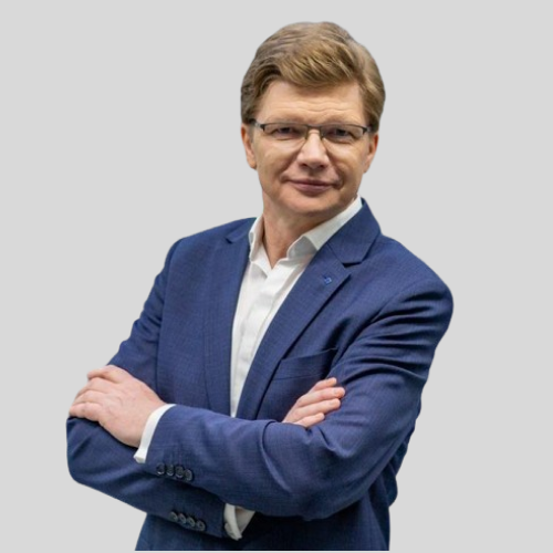
Salah Nasri
CEO and Co-Founder
International Semiconductor Industry Group (ISIG)
Salah Nasri is the CEO and Co-Founder of the International Semiconductor Industry Group (ISIG), a global organization founded in 2010 that connects and empowers semiconductor decision-makers through strategic leadership platforms, executive summits, and collaborative initiatives. ISIG has become a trusted global hub for industry leaders driving innovation and progress across the semiconductor value chain.
With extensive experience across the semiconductor sector, Salah has played a pivotal role in fostering global collaboration among industry leaders. Under his leadership, ISIG has evolved into one of the most influential communities in the semiconductor ecosystem—bringing together executives, innovators, and policymakers across regions including the United States, Europe, Asia, and the Middle East.
Salah has been instrumental in expanding ISIG’s reach and impact, curating high-level summits and initiatives that drive dialogue and progress across critical areas such as semiconductor manufacturing, AI, MEMS, automotive electronics, and advanced packaging. His vision continues to position ISIG as a key platform for thought leadership, networking, and strategic industry alignment.
Earlier in his career, Salah held positions at Credit Suisse, Goldman Sachs, Worldwide Business Research, and the International Business Development Group. He studied International Relations and Economics at Oxford University and Loughborough University, and in 2024 became a Stanford University alumnus after completing the Stanford Executive Program. In addition to his role at ISIG, Salah also serves on the Advisory Board of Atlant3D, a pioneer in atomic-layer advanced manufacturing solutions.
Company Profile
Established in 2010, the International SemiconductorIndustry (I.S.I.G.) is a prestigious & trusted associationwithin the semiconductor industry, renowned fororchestrating major regional summits across the globe,ranging from the U.S, the Middle East & Asia via ourdivision, the International Semiconductor ExecutiveSummits (I.S.E.S.). Our summits are fully endorsed bylocal governments and leading companies in all areas ofthe semiconductor supply chain.
Moreover, I.S.E.S. serves as the Premier platform for senior executives in technology, manufacturing, and R&D from diverse semiconductor companies, technology providers, and affiliated industries.
Our events are instrumental helping to shed light onto key industry trends, drive innovation and influence key decisions to help shape, and advance the growth of the semiconductor sector.
09:20 – 09:35
Huishan District People’s Government Promotion Speech 惠山区集成电路产业推荐
Jinfeng Ding 丁劲锋 无锡市惠山区高新技术企业协会副秘书长
09:35 – 09:55
Keynote
CRRC Automotive Power Semiconductor Technology Innovation and Industrialization 中车汽车功率半导体技术创新与产业化

Ding Rongjun
Academician of Chinese Academy of Engineering, Chief Engineer CRRC 丁荣军 院士 / 中车总工程师
CRRC
Ding Rongjun, Academician of the Chinese Academy of Engineering, expert in power electronics and control technology, recipient of the State Council Special Allowance; member of the National Industry Foundation Committee, Director of the National Key Laboratory of Power Semiconductors and Integrated Technology, Chairman of the Power Semiconductor Industry Alliance, and Editor-in-Chief of the academic journal Locomotive Electric Drive; representative of the 18th and 19th National Congresses of the Communist Party of China; currently serving as Chief Scientist of CRRC (China Railway Rolling Stock Corporation) and Dean of the School of Mechanical and Vehicle Engineering at Hunan University.
Academician Ding has long been engaged in innovative research and technology transfer in the fields of power electronic devices, traction converters, and AC drive systems. He established a standards system suited to China’s national conditions that aligns with international technical models. His contributions have played a significant role in China’s breakthrough development from conventional rail to heavy-duty rail and from regular-speed to high-speed rail. He has presided over or participated in more than 30 major national, provincial, and ministerial-level research projects, received 1 National Invention Award, 2 Second Prizes for National Scientific and Technological Progress, 3 Special Prizes, 8 First Prizes, and 4 Second Prizes at the provincial and ministerial levels. He has also been honored with the “Ho Leung Ho Lee Science and Technology Award,” “Zhan Tianyou Science and Technology Achievement Award,” “Mao Yisheng Science and Technology Award,” designation as a national-level talent in the “New Century Hundreds-Thousands-Talents Project,” and titles such as “National Model Worker,” “Most Beautiful Railway Technology Worker,” and one of the “50 Honored Figures of China’s Subway Development.”
丁荣军,中国工程院院士,电力电子及控制技术专家,国务院特殊津贴获得者;国家产业基础委员会委员、功率半导体与集成技术全国重点实验室主任、功率半导体行业联盟理事长、学术期刊《机车电传动》主编;中国共产党十八大、十九大代表;现任中国中车首席科学家,湖南大学机械与运载装备学院院长。
丁院士长期从事电力电子器件、牵引变流和交流传动系统的创新研究和成果转化,创建了适合我国国情的标准体系并与国际接轨的技术模式,为中国铁路从普载到重载、从常速到高速的突破发展做出了重大贡献。先后主持、参与国家、省部级重大科研项目30余项,获国家发明奖1项、国家科技进步二等奖2项、省部级特等奖3项、一等奖8项、二等奖4项,获“何梁何利科学技术奖”、“詹天佑科技成就奖”、“茅以升科学技术奖”、“新世纪百千万人才工程国家级人选”、“全国劳动模范”、“最美铁道科技工作者”和”中国地铁50年致敬人物“等荣誉称号。

Part1 Topic: Industry View from the analyst 行业分析师的观点
09:55 – 10:15
Keynote
Powering the Future: Innovations in Power Semiconductors for Vehicle Electrification and Beyond 驱动未来:汽车电气化与功率半导体创新发展报告

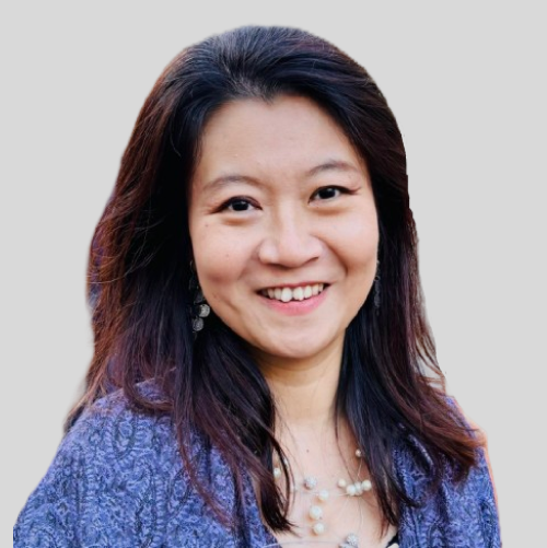
Yik Yee Tan, PhD
Senior Technology & Market Analyst, Semiconductor Packaging
Yole Group
Yik Yee Tan, PhD is Senior Technology & Market Analyst, Semiconductor Packaging at Yole Group.
Based in Malaysia, Yik Yee follows the semiconductor packaging industry and its evolution. Based on her technical expertise and market knowledge, she develops technology & market products and is engaged in dedicated custom projects.
Prior to Yole Group, Yik Yee Tan worked as a failure analyst and interconnect principal at Infineon Technologies (Malaysia) and later as an open innovation senior manager at onsemi (Malaysia). While at onsemi, Yik Yee was deeply involved in numerous innovative advanced packaging projects.
She authored more than 30 papers and wrote 3 patents related to semiconductor packaging technologies.
Yik Yee Tan holds a PhD in Engineering from Multimedia University (MMU, Malaysia).
Company Profile
Yole Group is a leading international market research and strategy consulting firm, delivering in-depth analyses across market trends, technology developments, teardowns, and reverse costing. Leveraging deep semiconductor expertise, its team of analysts also provides custom consulting services, offering strategic, technical, and market insights tailored to address specific business challenges and opportunities.
Janet Tang
Partner & Managing Director
AlixPartners
Janet brings 20 years of a variety of industry experience such as as chief strategy officer (CSO) of a Global 500 company, oversight of P&L responsibilities, service in consulting leadership, role as a software architect, and engagements in entrepreneurship. Janet is known for successfully driving complex transformations in technology firms and telcos, turning around cost centers into profit centers, building transformative go-to-market engines, and coaching next generations of client leaders. Her early career as a software architect in Silicon Valley also gave her hands-on experience in R&D and product management.
Janet has a Master of Science in Computer Science from Stanford University. She has served as a board member of the University of Toronto Engineering Alumni Network and as chair of the network’s Nomination and Governance Committee.
Company Profile
AlixPartners is a results-driven global consulting firm that specializes in helping businesses respond quickly and decisively to their most critical challenges—from urgent performance improvement to complex restructuring, from risk mitigation to accelerated transformation. These are the moments when everything is on the line—a sudden shift in the market, an unexpected performance decline, a time-sensitive deal, a fork-in-the-road decision. We stand shoulder to shoulder with our clients until the job is done, and only measure our success in terms of the results we deliver.
Company Products & Services
Clients call us when they need pragmatism and cut-through to solve their most complex challenges arising from a continually disrupted world. Our services cover Artificial Intelligence, Corporate Strategy & Transformation, Data Governance, ESG, Growth, Investigations, Disputes & Advisory Services, Mergers & Acquisitions, Organizational Transformation, Supply-Chain Management & Operations, Technology, Transformative Leadership and Turnaround and Restructuring.

10:30 – 11:15
Tea / Coffee Break Networking & Business Meeting 2 & 3 社交茶歇及贸易配对会 2&3
Part2 Topic: Insights from leading semiconductor companies shaping the Mobility landscape 全球领先的半导体领导者视野中的电动出 行
11:15 – 11:35
Keynote
Semiconductor Strategies for the Transition to Sustainable Energy and Mobility 向可持续能源和移动转型的半导体战略
Power technologies are pivotal in driving sustainability and achieving carbon neutrality. At the forefront of this revolution, innovative semiconductor solutions are propelling e-mobility and software-defined vehicles into the future. The demand for high-efficiency applications is pushing the boundaries of semiconductor technology, particularly those with wider bandgaps. Silicon carbide has emerged as a game-changer in car electrification and high-end industrial applications. ST is a leading innovator with major investments in R&D and manufacturing investment. With cutting-edge semiconductor solutions, ST is poised to meet the dynamic needs of a rapidly evolving marketplace.

Dino Costanzo
Application Director and head of Motor Control Competence Center in AP.
STMicroelectronics
Application Director, has 20 years of experience in application development, in the field of System solutions for Motor Control;
After graduated with a Master’s degree in Electric Engineering from the University of Catania, he joined STMicroelectronics Italy in 2006, where he was appointed Project Leader of STM32 Motor Control Firmware Library (MCSDK), and taking the role of coordination of the joint developments with Universities.
Later on, he moved in 2015 to Shenzhen, where he is now directing the Motor Control Competence Center of China and APeC regions, working on the development of advanced solutions for the industrial market, comprising HVAC, Servo Drives, and Power Tools.
His research interest are in algorithms for three-phase motors, where he is author of 7 US patents and others pending, in the fields of HFI sensorless control, acoustic noise reduction, motor currents reading, multiple Motor Control architectures, digital power etc.
Major customers in Asia have made partnership with his team, and generated successful product lines based on ST products and solutions, for which the Motor Control Competence Center has been awarded consecutively for “best motor control platform” by specialized reviews.
Company Profile
At ST, we are more than 50,000 creators and makers of semiconductor technologies mastering the semiconductor supply chain with state-of-the-art manufacturing facilities. An integrated device manufacturer, we work with more than 200,000 customers and thousands of partners to design and build products, solutions, and ecosystems that address their challenges and opportunities, and the need to support a more sustainable world. Our technologies enable smarter mobility, more efficient power and energy management, and the wide-scale deployment of cloud-connected autonomous things. We are committed to achieving our goal to become carbon neutral on scope 1 and 2 and partially scope 3 by 2027. Further information can be found at www.st.com.

11:35 – 11:55
Keynote
Infineon Enables Automotive Decarbonization and Digitization Development Infineon 助力汽车低碳化与数字化发展
INFINEON 英飞凌

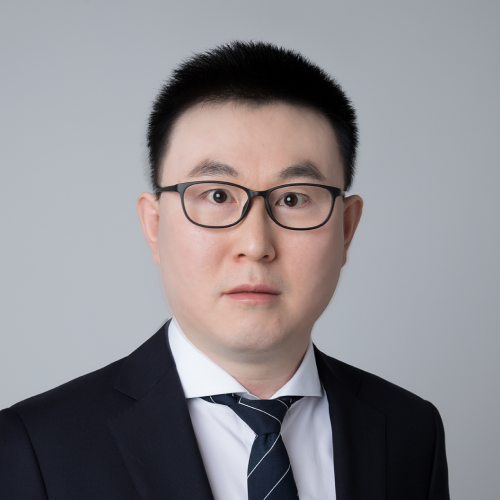
Gary Zhong
Senior Director and Head of Vehicle Motion Segment
Infineon Technologies AG
Gary Zhong joined Infineon as Head of Vehicle Motion Segment in the Greater China region in October 2020. Gary brings with him over 15 years of professional experiences in top new energy vehicle industry companies and demonstrated his strong technical background and leadership in NEV battery system, traction motor, and vehicle control areas.
Company Profile
Here at Infineon, we combine entrepreneurial success with responsible action to make life easier, safer, and greener. Barely visible, semiconductors have become an indispensable part of everyday life. We play a key role in shaping a better future – with microelectronics that link the real and the digital world. Our semiconductors enable efficient energy management, smart mobility, as well as secure, seamless communications in an increasingly connected world. Infineon designs, develops, manufactures and markets a broad range of semiconductors and system solutions. The focus of its activities is on automotive and industrial electronics, communication and information technologies, IoT, sensor technology and security. The product range comprises standard components, software, customer-specific solutions for devices and systems, as well as specific components for digital, analog, and mixed-signal applications.
11:55 – 12:15
Keynote
Bosch SiC Enable the Future Electric Mobility 博世SiC赋能未来电动出行
Introduce the Bosch Group’s SiC semiconductor business, the trench technology SiC chips. Introduce the power modules that Bosch developed dedicate for mass market new energy vehicles.
The power module on pin-fin cooler.
The Compact SiC Line (CSL)
Leadframe SiC Line (LSL)
介绍了博世集团SiC功率半导体的发展历程,重点介绍了博世集团针对新能源汽车电驱专门开发的碳化硅功率模块的主要特点和性能指标。
(1) 紧凑型碳化硅功率模块(CSL)
(2) 引线框架塑封碳化硅功率模块(LSL)
Dr. Richard Feng
Director of power semiconductor and module R&D center
Robert Bosch GmbH
Dr. Feng is the Director of power semiconductor and module R&D center at Bosch Mobility Electronics (ME) China, where he and his engineering team focus on the design, characterization, testing and application of innovative and cost-effective power semiconductor components and power modules for China and global EV market. The product portfolio includes SiC bare dies, IGBT and SiC power modules.
Dr. Feng boasts 10 years of experience in the application of SiC and GaN device. He has 6 years of experience on Electric Vehicle (EV) traction inverter power module research, development, and power module application in China car OEMs and Tier1suppliers.
Dr. Feng obtained his Ph.D. degree in Power Electronics from Zhejiang University China in 2004.
Company Profile
The Bosch Group is a leading global supplier of technology and services. It employs roughly 428,000 associates worldwide (as of December 31, 2023). According to preliminary figures, the company generated sales of 91.6 billion euros in 2023. Its operations are divided into four business sectors: Mobility, Industrial Technology, Consumer Goods, and Energy and Building Technology. As a leading IoT provider, Bosch offers innovative solutions for smart homes, Industry 4.0, and connected mobility. Bosch is pursuing a vision of mobility that is sustainable, safe, and exciting. It uses its expertise in sensor technology, software, and services, as well as its own IoT cloud, to offer its customers connected, cross-domain solutions from a single source. The Bosch Group’s strategic objective is to facilitate connected living with products and solutions that either contain artificial intelligence (AI) or have been developed or manufactured with its help. Bosch improves quality of life worldwide with products and services that are innovative and spark enthusiasm. In short, Bosch creates technology that is “Invented for life.” The Bosch Group comprises Robert Bosch GmbH and its roughly 470 subsidiary and regional companies in over 60 countries. Including sales and service partners, Bosch’s global manufacturing, engineering, and sales network covers nearly every country in the world. The basis for the company’s future growth is its innovative strength. At 136 locations across the globe, Bosch employs some 90,000 associates in research and development, of which roughly 48,000 are software engineers.
Tong Wu, Ph.D.
Leader of China Automotive Solution Team
onsemi
Dr. Tong Wu is leading the onsemi Automotive Application and Marketing team in China. He graduated from Shanghai Jiao Tong University with a bachelor in Semiconductor Physics, minoring in Mathematics, and holds a Ph.D. in Electrical Engineering from the University of Tennessee, USA. Dr. Wu has over 10 years of R&D and industrial experience in semiconductor packaging and the design and application of silicon carbide.
He is now responsible for automotive technology engagement in China, covering from product definition, manufacturing, marketing, to system applications. He maintains in-depth cooperation with multiple automotive OEMs and Tier 1 suppliers.
Dr. Wu previously worked at the Oak Ridge National Laboratory (ORNL) in Oak Ridge, Tennessee, USA, and also with solid industrial R&D backgrounds. He has published more than 40 papers in international conferences and journals and has also been granted multiple US patents in the field of semiconductors.
Company Profile
onsemi (Nasdaq: ON) is driving disruptive innovations to help build a better future. With a focus on automotive and industrial end-markets, the company is accelerating change in megatrends such as vehicle electrification and safety, sustainable energy grids, industrial automation, and 5G and cloud infrastructure. With a highly differentiated and innovative product portfolio, onsemi creates intelligent power and sensing technologies that solve the world’s most complex challenges and leads the way in creating a safer, cleaner, and smarter world.
12:35 – 13:45
Buffet Lunch & Business Meeting Networking 4 自助午餐 & 贸易配对会 4
13:45 – 14:30
Part 3 Panel : Synergy Driving Innovation in electrification & Mobility 圆桌讨论:协同驱动电气化与移动性创
Moderator
Salah Nasri
CEO and Co-Founder
International Semiconductor Industry Group (ISIG)
Salah Nasri is the CEO and Co-Founder of the International Semiconductor Industry Group (ISIG), a global organization founded in 2010 that connects and empowers semiconductor decision-makers through strategic leadership platforms, executive summits, and collaborative initiatives. ISIG has become a trusted global hub for industry leaders driving innovation and progress across the semiconductor value chain.
With extensive experience across the semiconductor sector, Salah has played a pivotal role in fostering global collaboration among industry leaders. Under his leadership, ISIG has evolved into one of the most influential communities in the semiconductor ecosystem—bringing together executives, innovators, and policymakers across regions including the United States, Europe, Asia, and the Middle East.
Salah has been instrumental in expanding ISIG’s reach and impact, curating high-level summits and initiatives that drive dialogue and progress across critical areas such as semiconductor manufacturing, AI, MEMS, automotive electronics, and advanced packaging. His vision continues to position ISIG as a key platform for thought leadership, networking, and strategic industry alignment.
Earlier in his career, Salah held positions at Credit Suisse, Goldman Sachs, Worldwide Business Research, and the International Business Development Group. He studied International Relations and Economics at Oxford University and Loughborough University, and in 2024 became a Stanford University alumnus after completing the Stanford Executive Program. In addition to his role at ISIG, Salah also serves on the Advisory Board of Atlant3D, a pioneer in atomic-layer advanced manufacturing solutions.
Company Profile
Established in 2010, the International SemiconductorIndustry (I.S.I.G.) is a prestigious & trusted associationwithin the semiconductor industry, renowned fororchestrating major regional summits across the globe,ranging from the U.S, the Middle East & Asia via ourdivision, the International Semiconductor ExecutiveSummits (I.S.E.S.). Our summits are fully endorsed bylocal governments and leading companies in all areas ofthe semiconductor supply chain.
Moreover, I.S.E.S. serves as the Premier platform for senior executives in technology, manufacturing, and R&D from diverse semiconductor companies, technology providers, and affiliated industries.
Our events are instrumental helping to shed light onto key industry trends, drive innovation and influence key decisions to help shape, and advance the growth of the semiconductor sector.
Panelist
Tim Yeh, Ph.D.
Technical Director
Sanan Semiconductor
Tim Yeh holds a Ph.D. in Electrical Engineering from National Central University in Taiwan and serves as a member of the Executive Advisory Committee of the International Semiconductor Executive Summit (ISES China). He has long been engaged in the research and industrialization of compound semiconductor materials and devices, with 25 years of industrial R&D experience, particularly in the field of third-generation semiconductor materials and devices. He is well-versed in the design and industrial manufacturing of compound semiconductor devices.
Dr. Ye has previously worked as a researcher at the Telecommunication Laboratories of Chunghwa Telecom in Taiwan and served as a technical director for a publicly listed company in Taiwan. His research achievements have led to the granting of more than 30 patents across the United States, Japan, Mainland China, and Taiwan, and he has published over 70 papers in international journals. He has led or participated in several major projects under China’s Ministry of Science and Technology and key national R&D programs.
He currently serves as the Technical Director at Hunan Sanan Semiconductor, where he is responsible for the R&D and mass production integration of compound semiconductor power electronic devices. He has successfully established a full industrial chain production line for third-generation semiconductor power electronic devices, covering the entire process from epitaxy to device fabrication.
叶念慈,台湾中央大学电机工程博士,国际半导体高管峰会 (ISES China)执行顾问委员会成员,长期从事化合物半导体材料和器件研究及产业化,特别是在 第三代半导体材料和器件 领域拥有 25 年的产业研发经验,精通化合物半导体器件设计和产业化制造。曾先后任台湾中华电信公司电信研究所研究员及台湾上市公司技术负责人。研究成果获美国、日本、中国大陆和台湾地区专利授权30 余件,发表国际期刊论文 70 余篇,曾作为项目或课题负责人参与数项国家科技部重大专项和国家重点研发计划项目。现担任湖南三安半导体技术总监,负责 化合物半导体功率电子器件研发与量产导入,成功打造从外延到器件全产业链 第三代半导体功率电子器件产线。
Company Profile
Sanan Semiconductor is a wholly-owned subsidiary of the listed company Sanan Optoelectronics. Sanan is committed to becoming a world-class R & D, manufacturing and service platform for wide bandgap semiconductors. Sanan Semiconductor extended Sanan Optoelectronics’ 20-year compound semiconductor industrialization experience to the field of power electronics, and became a full-chain integration platform focusing on the wide bandgap semiconductor industry and providing the most comprehensive products and services.
Company Products & Services
Sanan Semiconductor’s silicon carbide (SiC) power products include automotive and industrial SiC Schottky barrier diodes (SBD) and SiC MOSFETs which provide key components with higher power density and higher energy conversion efficiency for the electric vehicles and renewable energy markets. These can then be applied to high-reliability applications such as electric vehicle drivetrains, charging stations, and solar photovoltaic inverters. Sanan Semiconductor is a member of the JEDEC JC-70 Wide Band Gap Semiconductor Standards Committee, which collaborated with the industry to provide process technologies and products with improved reliability and quality. The company also has a portfolio of AEC-Q101 certified products.

Panelist
Wei Wang
Director of BD
Automotive Research Institute (Suzhou), Tsinghua University (TSARI)
Career
- 2016 – now Assistant president 、 Director of R&D and Operation in TSARI
- 2011 – 2016 General manager in MicRiver Information Systems
- 2001- 2010 AP Manager, BP, PM in Delphi Packard Electric Systems
Study
Graduated from Automotive Engineering Department of Tsinghua University in 1999, and Olin Business School of Washington University in St. Louis in 2008.
Other information
Senior engineer in management domain; Member of JS-SAE automobile intelligent manufacturing committee & Industry Standard Committee of Automotive Intelligent Manufacturing
Company Profile
Tsinghua University Suzhou Automotive Research Institute was established in 2011. It is the first specialized research institute of Tsinghua University for a specific industry. It is also a comprehensive automotive industry research institute jointly built by Tsinghua University and Suzhou Municipal Government. It is committed to the research and development of automotive application technology, transformation of scientific and technological achievements and incubation of high-tech enterprises.
Relying on the technical and talent advantages of Tsinghua University, guided by the major needs of the country and the industry, and with the mission of “leading technological innovation and promoting industrial progress”, we focus on new industries such as intelligent connected vehicles and new energy vehicles, and have established six business platforms: technology research and development, analysis and testing, science and technology finance, talent training, technology transfer, and enterprise incubation. We lead the innovative development of the industry with the research and development of new technologies and new products and industrial transformation, and promote industrial transformation and upgrading with technology, finance and talent services.
We have gradually built a comprehensive industrial innovation platform integrating scientific and technological innovation, industrial services and entrepreneurial incubation functions, forming an innovative industrial ecology where high-end talents gather, science and technology finance is active, and high-tech enterprises gather.

Panelist
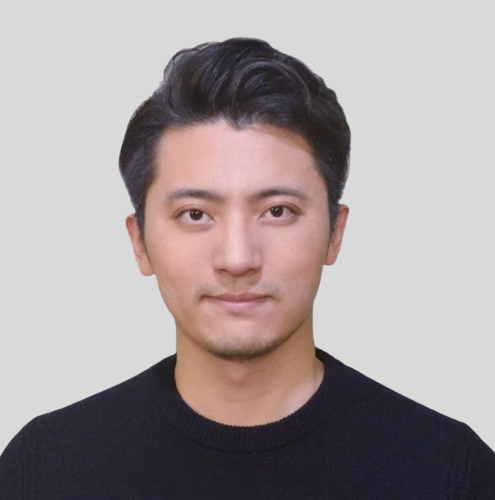
Jason Wang
Founder
Joinsilicon
Hongpeng Wang graduated from the Department of Electronic Engineering of Tsinghua University with Bachelor and Master degree. He has worked in many well-known chip design companies as the head of R&D, and has more than 15 years of technical management experience. He is an expert in IC design and system architecture, and has successfully mass-produced 20+ chips for different applications.
In 2021, he founded Join Silicon. Join Silicon is a technology platform company focusing on IC design of advanced process technology, committed to IP independent R&D and service, enabling chip design and SoC customized solutions. Join Silicon provide advanced process IP, one-stop high-end SoC customization, as well as chiplet and advanced 2.5D/3D packaging products for customers in high-performance computing, data center, 5G communications, artificial intelligence, automotive electronics etc..
Company Profile
JoinSilicon is a world class Product Engineering Company that provides custom products and solutions for the semiconductor industry. Our large pool of well-trained engineers can support from Application Software to Transistor Level Layout in advance technology nodes including 6nm. Customers take advantage of our extensive experience in co-developing hardware and software under one roof to translate their ideas into real products. Our turnkey ASIC engagement model allows our customers to rely on warranties provided on work performed. With the experience of shipping millions of production worthy silicon to customers, JoinSilicon, is your trusted partner to deliver designs on time with the quality you expect.

Panelist
Vishnu Kumaresan, Ph.D
Semiconductor Business Specialist & Segment Leader
Volvo Group
Vishnu Kumaresan as a Segment Leader drives Volvo Group’s Semiconductor strategy. He has a doctorate degree in semiconductor field and has specialized in strategy development. Vishnu has more than 10 years of experience in the semiconductor, software, and display technologies before joining Volvo group.
Company Profile
The Volvo Group is one of the world’s leading manufacturers of trucks, buses, construction equipment and marine and industrial engines. The Group also provides complete solutions for financing and service. The Volvo Group, with its headquarters in Gothenburg, employs about 100,000 people, has production facilities in 18 countries and sells its products in more than 190 markets.

Panelist
Damon Tsai
Head, Product Marketing
Onto Innovation
Damon Tsai boasts over 14 years of extensive experience in inspection and metrology within the semiconductor equipment industry. With a specialized focus on semiconductor FEOL, advanced packaging and specialty markets like SiC, GaN, RF, and CIS, Damon joined Onto Innovation in 2018. Serving as the leader of the global inspection product marketing team, he has been instrumental in shaping product strategy for business growth. Currently, Damon leads the inspection product marketing team at Onto Innovation, overseeing roadmap development and product line strategy to align with market demands.
Prior to Onto Innovation, Damon held the position of Asia product director of the inspection BU at Ultratech (now Veeco). In this role, he managed in-line 3D wafer shape measurement for VNAND/DRAM/Logic process control. Damon collaborated closely with leading foundry and memory customers, contributing to the development of feedforward overlay control for next-generation lithography technology and in-line process control to enhance yield. His earlier experience at KLA involved working as a product marketing manager, where he focused on defect inspection for compound semiconductors, SiC, GaN and GaAs. Notably, he has a strong academic presence, having published over 20 technical papers/articles in public forums.
Company Profile
Onto Innovation is a leader in process control, combining global scale with an expanded portfolio of leading-edge technologies that include: Un-patterned wafer quality; 3D metrology spanning chip features from nanometer scale transistors to large die interconnects; macro defect inspection of wafers and packages; elemental layer composition; overlay metrology; factory analytics; and lithography for advanced semiconductor packaging. Our breadth of offerings across the entire semiconductor value chain helps our customers solve their most difficult yield, device performance, quality, and reliability issues. Onto Innovation strives to optimize customers’ critical path of progress by making them smarter, faster and more efficient. Headquartered in Wilmington, Massachusetts, Onto Innovation supports customers with a worldwide sales and service organization.
General Telephone: +1 978 253 6200
General email: info@ontoinnovation.com
Website: www.ontoinnovation.com

Panelist
Changlin Pang
Platform Integration Lead
InchFab
Changlin Pang, PhD., Platform Integration Lead of InchFab Inc., received the B.S. and M.S. degrees in Precision instruments from Tsinghua University, China in 2002, and his M.S. and Ph.D. degrees in Electrical Engineering from Caltech with his Ph.D. project of polymer neural electrodes for a neural prosthesis system in 2007. Dr. Pang invented the world’s smallest implantable programmable ocular drug delivery pump for AMD treatment, started Replenish, Inc. which was invested by Alcon in 2008. He later joined Alcon for commercializing this micropump in 2015. Dr. Pang was the Co-founder and CTO of Golden Eye Bionics from 2017 to 2024 to develop and commercialize a new generation of retinal prosthesis products. Dr. Pang has more than 50 approved and pending patent applications.
Company Profile
InchFab pioneered Application Specific Fabs for the new era of chips, delivering the world’s only drop-in, ready-to-use modular fabrication lines with as short as 6-month delivery lead times. These $1-10M agile fabs enable state-of-the-art wafer processing at a fraction of traditional $1B+ costs. The company provides complete solutions including turnkey process flows, comprehensive education courses, and foundry services. By combining low CapEx, scalable throughput, and a proprietary process library, InchFab democratizes semiconductor manufacturing for workforce development, rapid prototyping, and production across specialized chips, non-IC devices, and localized supply chains.RetryM
Company Products & Services
Application Specific Fabs
Part 4 Topic: Automotive Innovations Challenges & Differentiation 汽车创新的挑战与差异化
14:30 – 14:50
Keynote
Opportunities in Commercial Vehicle Decarbonization 商用车辆的低碳机遇
Vishnu Kumaresan, Ph.D
Semiconductor Business Specialist & Segment Leader
Volvo Group
Vishnu Kumaresan as a Segment Leader drives Volvo Group’s Semiconductor strategy. He has a doctorate degree in semiconductor field and has specialized in strategy development. Vishnu has more than 10 years of experience in the semiconductor, software, and display technologies before joining Volvo group.
Company Profile
The Volvo Group is one of the world’s leading manufacturers of trucks, buses, construction equipment and marine and industrial engines. The Group also provides complete solutions for financing and service. The Volvo Group, with its headquarters in Gothenburg, employs about 100,000 people, has production facilities in 18 countries and sells its products in more than 190 markets.
14:50 – 15:10
Keynote
The Layout of Electric Drive and High Voltage System in NIO 蔚来在电驱及高压系统的布局
NIO is a globally leading tech company, and electric drive and high-voltage system is one of the 12 full-Stack technologies. NIO has developed four generation EDS, the latest 900V EDS shows higher performance, more compact and more intelligent: In-house design SiC power module and power stack enable extremely high power density ; Innovative electronic and software design enable boost charger function with high power and high voltage range ; AI based EDS technology empowering vehicles to be more Smart, Safe, and Efficient .
蔚来是全球领先的科技公司,电驱及高压系统就是12个全栈自研技术之一。蔚来已经开发了四代电驱系统,最新的900V电驱系统展示了更高的性能,更紧凑以及更智能:自研功率模块和逆变器极大提升了功率密度;创新性的软硬件设计使得系统可以在更宽电压范围内实现更高功率的充电功能;AI 在电驱系统的应用使得整车更加聪明、更加安全更高效。
Wilson Hong
Senior Director, Power Electronics Design Department & Senior Expert, ECU Product Engineering
Formerly Senior Director, responsible for all HV components’ development in NIO, incl. PEU, DCDC, OBC, HV harness etc. Leading Person Award in electric vehicle industry of Anhui Province China. Over 16 years of working experience in electric drive and high voltage system, holds over 50 patents in CN, EU and US. Win the first Prize of Science and Technology Progress of China Association of Automobile Manufactures in 2021.
Part 5 Topic: Energy Solutions for Tomorrow 未来能源解决方案
15:10 – 15:30
Keynote
Technology Innovation of ROHM’s Power Devices ROHM电源设备的技术创新
1)ROHM Group Corporate Profile
2)Medium-Term Management Plan
(Focusing on Analog LSIs and Power Devices)
3)Growth Strategy of SiC Power Devices
4)Growth Strategy of GaN Power Devices
1)ROHM集团公司概况
2)中期管理计划(专注于模拟LSI和电源设备)
3)SiC功率设备的增长战略
4)GaN功率设备的增长战略

Jun Li
General Manager (FAE Head Quarter), Shanghai
ROHM Semiconductor
JUNLI joined ROHM in 2003, and have been in charge of ROHM China Technical Center for almost 20 years, including applications and promotions of ROHM semiconductors in consumers, automobile and industry.
Company Profile
ROHM, a leading semiconductor and electronic component manufacturer, was established in 1958. From the automotive and industrial equipment markets to the consumer and communication sectors, ROHM supplies ICs, discretes, and electronic components featuring superior quality and reliability through a global sales and development network. Our strengths in the analog and power markets allow us to propose optimized solutions for entire systems that combine peripheral components (i.e., transistors, diodes, resistors) with the latest SiC power devices as well as drive ICs that maximize their performance.

15:30 – 15:50
Keynote
From Prototyping to Advanced Manufacturing of Sensors and Optical Components for Automotive Applications. 从原型设计到汽车应用中传感器和光学元件的高级制造。

Maksym Plakhotnyuk, Ph.D.
CEO & Founder
ATLANT 3D
Dr. Maksym Plakhotnyuk, is the CEO and Founder of ATLANT 3D, a pioneering deep-tech company at the forefront of innovation, developing the world’s most advanced atomic-scale manufacturing platform. Maksym is the inventor of the first-ever atomic layer advanced manufacturing technology, enabling atomic-precision development of materials, devices, and microsystems. A scientist with a Ph.D. in Nanotechnology, he has deep expertise in nanotechnologies, renewable and exponential technologies, semiconductor processing, solid-state physics, and material science. A Fulbright scholar, Hello Tomorrow Grand Winner, and proud Ukrainian, Maksym has earned global recognition for his work.
Company Profile
ATLANT 3D has mastered control of matter at the atomic scale, ushering in a new era in manufacturing. For research teams and manufacturers working at the frontiers of technology, we’ve created what was once thought unattainable: a system that builds materials and devices, atom by atom, with unprecedented precision and speed.
While others are constrained by traditional manufacturing limits, our breakthrough technology makes it possible to create the seemingly impossible, from next-generation quantum computers to devices that can operate in the harsh conditions of space. By replacing complex, resource-heavy processes with precise atomic-scale fabrication, we’re transforming technology while making manufacturing sustainable. We’re providing innovative teams the power to build technologies today that will define tomorrow’s world, using fewer resources to achieve greater possibilities.
Based in Copenhagen and London, with operations in the US, ATLANT 3D partners with research institutions and industrial companies to expand the boundaries of technological possibility.
Company Products & Services
ATLANT 3D is redefining microfabrication with its patented Direct Atomic Layer Processing (DALP®) technology. Our NANOFABRICATOR™ platform enables localized atomic layer processing for rapid material discovery, prototyping, and scalable device fabrication—bridging the gap from lab to fab.
Beyond hardware, we offer Pilot Projects and Joint Development Services to validate new materials and device architectures. A-HUB, our Microfabrication-as-a-Service (MaaS) centre, provides R&D teams with atomic-scale precision without the need for costly infrastructure.
From concept to fabrication, ATLANT 3D partners with academia and industry to drive next-generation innovations beyond conventional limits.

15:50 – 16:10
An OSAT Perspective of the Power Semiconductor Market OSAT对电力半导体市场的视角
Amkor 安靠
When talking about the power semiconductor market, most outsiders would describe it with words like “mature”, “stable” and “simple” compared to the mobile and digital semiconductor markets. One look from the inside will tell you this is not true. With the continued adoption of Wide Band Gap (WBG) materials along with the market forces driving electrification and renewable energy, you will see that power is anything other than “simple”.
Power semiconductors are becoming increasingly important in the overall semiconductor supply chain and innovations need to keep pace with the need for clean, efficient, and higher power delivery. Although innovations in power generally follow the smaller/better/faster/cheaper engine that continues to drive the semiconductor industry, some interesting dynamics are depending on the application and target market. The traditional market wants to standardize, and the new applications value optimization. These competing forces can create havoc from a supply chain standpoint, and as the power semiconductor market trends towards increasing complexity, then manufacturing strategies will need to adapt. From an OSAT perspective, this presents both a challenge and an opportunity.
This presentation will discuss three key areas of the market from an OSAT perspective and look at lessons learned from past events in our industry to give us some insight into what the supply chain might look like as both WBG devices and power foundry services continue to grow with demand from automotive, industrial, compute and commercial applications.
在谈到电力半导体市场时,大多数外部人士会用“成熟”、“稳定”和“简单”这些词来形容,与移动和数字半导体市场相比。然而,从内部来看,这种描述并不准确。随着宽禁带(WBG)材料的持续采用以及推动电气化和可再生能源的市场力量,你会发现电力半导体远非“简单”。
电力半导体在整个半导体供应链中变得越来越重要,创新需要跟上清洁、高效和更高功率传输的需求。尽管电力半导体的创新通常遵循更小/更好/更快/更便宜的引擎,这种引擎继续推动半导体行业的发展,但根据应用和目标市场的不同,一些有趣的动态也会出现。传统市场希望标准化,而新应用则重视优化。这些相互竞争的力量可能会从供应链角度造成混乱,随着电力半导体市场趋势变得越来越复杂,制造策略也需要适应。从OSAT(外包半导体组装和测试)角度来看,这既是一个挑战,也是一种机遇。
本次演讲将从OSAT的角度讨论市场的三个关键领域,并通过回顾我们行业中的过往事件,提供一些见解,以预测当WBG器件和电力代工服务随着汽车、工业、计算和商业应用的需求不断增长时,供应链可能会是什么样子。
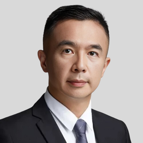
Troy Lin
Director, Product Marketing
Amkor Technology, Inc.
Troy joined Amkor in 2021 and is currently responsible for Global Product Marketing, Market Analytics and Market Strategy. Prior to joining Amkor, Troy has held various sales management, business development and customer engineering positions at Texas Instruments, Qualcomm, Arm and Google. Troy holds a BSE degree in Electrical Engineering and MSE degree in Biomedical Engineering from University of Michigan at Ann Arbor.
Troy 于 2021 年加入 Amkor,目前负责全球产品营销、市场分析和市场战略。在加入 Amkor 之前,Troy 曾在德州仪器 (TI)、高通 (Qualcomm)、安谋 (Arm) 和 (Google) 担任过销售管理、业务开发和客户工程职位。 Troy 拥有密歇根大学安娜堡分校的电气工程学士学位和生物医学工程硕士学位。
Company Profile
Amkor Technology, Inc. is the world’s largest US headquartered OSAT (outsourced semiconductor assembly and test). Since its founding in 1968, Amkor has pioneered the outsourcing of IC packaging and test services and is a strategic manufacturing partner for the world’s leading semiconductor companies, foundries, and electronics OEMs. Amkor provides turnkey services for the communication, automotive and industrial, computing, and consumer industries, including but not limited to smartphones, electric vehicles, data centers, artificial intelligence and wearables. Amkor’s operational base includes production facilities, product development centers and sales and support offices located in key electronics manufacturing regions in Asia, Europe and the United States. Learn more at https://amkor.com

16:10 – 16:55
Tea/Coffee Break Networking & Business Meetings 5&6 社交茶歇及贸易配对会 5&6
16:55 – 17:15
Keynote
High Voltage SiC MOSFET for renewable energy application with simpler design and higher power density 高电压SiC MOSFET用于可再生能源应用,具有更简单的设计和更高的功率密度。
WeEn Semiconductors 瑞能
As the renewable energy market grows, more and more companies are trying to simplify the inverter design from three-level to two-level topology. With SiC MOSFETs with higher breakdown voltage up to 2200V, two-level inverters are made possible. These 2200V SiC MOSFETs employ the latest technologies with smaller pitch size and better packaging technology with better thermal performance, and can help increase the power density with lighter system weight.
随着可再生能源市场的增长,越来越多的公司试图将逆变器设计从三电平简化为两电平拓扑。借助高达2200V的SiC MOSFETs,这种两电平逆变器变得可行。这些2200V的SiC MOSFETs采用了最新的技术,具有更小的间距尺寸和更好的封装技术,提供了更优的热性能,能够提高功率密度并减轻系统重量。
Kevin Shen
Chief Strategy & Business Operation Officer
WeEn Semiconductors
Kevin Shen is in charge of Corporate Strategy & Business Operation, CS&BO, which includes defining WeEn’s corporate strategy, driving our KPI tracking, pushing for our process improvements and heading the innovation programs with a focus to establish new platforms and address new market segments. Kevin graduated from Peking University, major in Physics. He has 17 years’ experiences in semiconductors and high tech companies, including NXP Semiconductors, Intel and Accenture. Most recently, he was responsible for China business in Leap Motion, a leading AR/VR technology company based in US.
Company Profile
WeEn Semiconductors Co., Ltd was registered as a company on Aug 5, 2015. WeEn’s global footprint has an operational headquarter in Shanghai and wholly owned subsidiaries and centers in Jilin (North East China, Front-End Fabrication) , Hong Kong, Manchester (Research and Development) , Dongguan (Warehouse and Distribution), and cities throughout the world (Sales Offices and Customer Service Access). In September 2018, WeEn added its new, in-house, reliability and failure analysis laboratory in Nanchang, Jiangxi Province, China. With a heritage of over 50 years in semiconductor development and manufacturing, WeEn as a key player has focused on developing a wide and deep portfolio of industry-leading power products including Silicon Carbide Power Devices, Silicon Controlled Rectifiers and Triacs, standard and fast recovery Power Diodes, TVS and ESD Diodes and IGBT and Modules. All these products are widely used in the markets for telecommunications, computing, consumer electronics, intelligent home appliances, lighting, automotive and power management applications. WeEn seeks to help our customers achieve improved cost and production efficiency and contribute to the development of global intelligent manufacturing.
瑞能半导体科技股份有限公司,注册于2015年8月5号,运营中心落户上海,全资子公司和分支机构,包括吉林芯片生产基地,香港子公司,上海和英国产品及研发中心,东莞物流中心,以及遍布全球其他国家的销售和客户服务点。2018年9月,瑞能半导体可靠性测试实验室及失效分析实验室在江西省南昌市正式开业, 可以对包括二极管,三极管以及可控硅等分立器件产品进行可靠性测试以及失效分析。自诞生以来,瑞能已走过逾 50 年辉煌历程。作为全球功率半导体行业的佼佼者,瑞能始终专注于研发行业领先、广泛且深入的功率半导体产品组合,公司主要产品主要包括碳化硅器件,可控硅整流器和晶闸管,快恢二极管,TVS,ESD,IGBT,模块等。产品广泛应用于以家电为代表的消费电子、以通信电源为代表的工业制造、新能源及汽车等领域。瑞能始终以优化客户体验,提升运营效率,强化核心技术为目标,推动全球智能制造行业的向前发展.
17:15 – 17:20
Mastering Plasma Technology Application – focus on local support for the semiconductor industry 掌握等离子体技术应用 – 专注于半导体行业的本地支持
TRUMPF Huettinger establishes provider for process power solutions with engineering and service centers throughout the world. Developing cutting-edge technology and high-end industrial solutions, with a global production footprint in Europe and Asia, we are focusing on customer closeness to enable for best-in-class support.
TRUMPF Huettinger 在全球设立了提供工艺电源解决方案的工程和服务中心。我们致力于开发尖端技术和高端工业解决方案,在欧洲和亚洲拥有全球生产基地,重点关注客户的需求,以提供一流的支持。
Pawel Ozimek, Ph.D EE
CTO, TRUMPF Huettinger and Managing Director, TRUMPF Huettinger Poland
TRUMPF Huettinger
Born in Warsaw, Poland. Studied Electrical Engineering at the Warsaw University of Technology and in 2006 he obtained a PhD in 2006 for the thesis entitled: “A new concept of a power supply system for auxiliary systems in the power industry”.
He started his career in 1995 in APS Energia team, on the basis of which Advanced Converters grew – a company founded to develop and provide power supplies for plasma processing. He actively participated in the process of merging the Advanced Converters with TRUMPF Huettinger. For many years he held the position of CTO responsible for RnD, Service and Marketing of TRUMPF Huettinger in Poland. In 2019 he was appointed Managing Director of the Polish branch.
Dr. Ozimek is an author and co-author of many power electronics solutions used in TRUMPF Huettinger’s products. He has been granted several patents in area of power supplies for plasma applications. Throughout his professional career, he has been actively promoting knowledge in the field of power electronics and its application for plasma processing as an author of many publications and a speaker at scientific conferences.
Company Profile
通快霍廷格电子有限公司成立于1922年,总部设于德国弗莱堡,是世界领先的等离子体电源制造商,产品主要用于:半导体,显示器和太阳能领域,以及光学镀膜,装饰镀膜,工业镀膜,大面积玻璃镀膜等行业的等离子体应用,于1990年正式加入通快集团。通快霍廷格电子致力于开发、制造用于各种沉积和干法刻蚀工艺的等离子电源,在电源领域拥有一百多年的经验积累,在欧洲、美洲和亚洲分别设有销售和服务子公司和分支机构。
2006年,通快霍廷格电子中国成立,至今已经深耕中国市场19年。如今,通快霍廷格在中国设有亚太区应用中心、维修中心、电源及匹配器生产中心,为客户提供所有生产过程中的优质服务。2023年,通快霍廷格中国新工厂在太仓建成开业,这是通快霍廷格继德国、波兰之后布局的全球第三家生产制造基地。
TRUMPF Huettinger is a high-tech company and a leading global manufacturer of DC, medium-frequency, high-frequency and semiconductor-based solid-state microwave generators.
The business units include plasma technology, industrial heating, battery inverter systems as well as microwave generators and amplifiers. These process power supplies are being used in many key processes in research, development and production. As a part of TRUMPF – technology leader of industrial lasers and machine tools – TRUMPF Electronics is headquartered in Freiburg/Germany and has sales and service branches in Europe, US and Asia providing a global IoT based service support.
Company Products & Services
Product introduction:
1. TruPlasma DC 4000 (G2) Series
TruPlasma DC 4000 (G2) 系列专为金属,金属氧化物,绝缘材料的反应直流溅射而开发。电源以直流脉冲的形式输出,在高要求的膜层质量和大产能的PVD 和PECVD 工艺中证明了它的优势。
The TruPlasma DC Series 4000 (G2) combines the excellent arc handling of TRUMPF Hüttinger with the advantages of DC pulse technology. This means you gain improved coating results with fewer defects, along with a higher deposition rate. The results are brilliant surfaces and a high level of production power.
2. TruPlasma DC 3000 (G2) Series
TruPlasma DC 3000 (G2) 系列适合众多直流溅射工艺,得益于先进的电弧管理和集成水冷装置,该款直流电源同样可用作脉冲式直流电源的高性价比替代方案。此外,极其紧凑的结构使其方便集成至现有应用中。
The TruPlasma DC Series 3000 (G2) is suited to numerous DC sputtering processes. The DC generators also make an interesting cost-effective alternative to pulsed DC generators due to their progressive arc management and the integrated water cooling. The very compact design also enables simple integration into existing applications.
3. TruPlasma RF 1000/3000 (G2/13) Series
全新一代的射频电源TruPlasma RF 1000 / 3000 (G2/13.56M) 系列,对工艺过程中的所有参数进行实时监测,即使在要求严苛的等离子体工艺中,仍能确保可靠供电。其稳定的输出功率和高精度控制确保高效高生产效率的同时,实现最佳工艺效果。
The TruPlasma RF Series 1000 / 3000 (G2/13) are the latest generation of RF generators. Due to innovative functions such as the patented CombineLine coupling technology or real-time measurement of all process parameters, reliable power supply even in demanding plasma processes is guaranteed – the optimal conditions for reproducible results and high productivity.
4. TruPlasma LF Series
TruPlasma LF 1000 系列电源基于创新的平台概念, 频率范围有350k,400k,2M,功率范围1~10kw,适用于各类半导体,光伏,ALD,刻蚀等离子应用。
TruPlasma LF 1000 series are based on an innovative platform concept with frequency ranges of 350k, 400k, 2M and power ranges from 1 to 10kw for all types of semiconductors, photovoltaic, ALD, and etch plasma applications.
5. TruPlasma VHF 3000 series
TruPlasma VHF 3000 系列电源基于创新的平台概念, 频率覆盖27M;40M;60M。功率范围1~10kw。可满足极为苛刻的生产要求。VHF 电源的纯水冷模块化结构与极高的功率密度设计可以确保大功率输出下的稳定性。
TruPlasma VHF 3000 series power supply is based on an innovative platform concept covering frequencies of 27M, 40M, 60M, and power ranges of 1~10kw to meet the most demanding production requirements. the VHF power supply’s pure water-cooled modular construction and extremely high power density design ensure stability at high power outputs.

Part 6 Equipment / Materials Suppliers Update 设备/材料供应商新趋势 发布
17:20 – 17:30
Electroless Metallization of power semiconductor devices – challenges and benefits 功率半导体器件的化学镀金属化—挑战与机遇
In today’s world with its increasing demand in power semiconductor devices for electrification, e-mobility and enabling the flexible use of green energy it has become more and more imminent that it is not only necessary to involve new semiconductor materials (e.g. SiC, GaN) but also apply alternative manufacturing technologies to maintain the flexibility and reliability on the next generation of power semiconductor devices.
Electroless metallization processes from MKS are part of these alternative technologies for power semiconductor device manufacturing and have been established in the industry over past 10 years with their benefit of providing maskless metallization with higher throughput capability at a reduced Cost of Ownership compared to physical metallization techniques. Usually, electroless processes are being used as final finish on Cu or Al-based substrates but there is also the possibility of direct metallization of semiconductor material (e.g. Si, SiC, GaN) using the electroless processes and create a reliable ohmic contact
在当今世界,随着电气化、电动汽车以及实现绿色能源的灵活应用,对功率半导体器件的需求在不断增加。为保持下一代功率半导体器件的灵活性和可靠性,越来越紧迫是,不仅需要应用新的半导体材料(例如SiC、GaN),而且需要应用替代制造技术。
MKS公司的化学镀金属化工艺是用于功率半导体器件制造的这些替代技术的一部分,并且已经在该行业中应用超过了十年。其自对准金属化的优点与物理金属化技术相比,具有更高的产能和更低的生产成本。通常,化学镀工艺被用于铜基或者铝基的最终处理;另外还有一种可能性,就是在半导体材料(例如Si、SiC、GaN)表面直接用化学镀工艺沉积金属以形成一个可靠的欧姆接触。

Dr. Stefan Pieper
Global Application Manager
mks | Atotech
Stefan Pieper has studied chemistry in Berlin, Germany where he also completed his PH.D. in analytical chemistry. In 2009 he joined Atotech as Application Scientist in the department of Semiconductor Advanced Packaging processes where he used the opportunity to gain deep insight in multiple electrochemical metallization processes and their characterization for semiconductor application. During his work as Application Scientist, he also spent over 3 years in the US where he optimized Cu dual damascene electrodeposition and Through Silicon Via plating. In 2020 he took over the position of Global Application Manager for Electroless deposition processes in semiconductor application at Atotech. In his current position he is leading a team that provides wet-chemical solutions for semiconductor metallization with the focus on power semiconductor.
Stefan Pieper博士曾在德国柏林学习化学,并在那里获得分析化学博士学位。2009年,他加入安美特,担任半导体先进封装工艺部应用科学家。利用这个机会,他深入了解了多种电化学金属化工艺及其在半导体应用中的特性。在担任应用科学家期间,他还在美国花了3年多的时间,优化了双大马士革铜互连工艺和硅通孔电镀工艺。2020年,他接任安美特半导体化学镀工艺全球应用经理一职。在目前的职位上,他领导的团队为半导体金属化提供湿制程解决方案,重点是功率半导体。
Company Profile
Atotech, a brand within the Materials Solutions Division of MKS Instruments, develops leading process and manufacturing technologies for advanced surface modification, electroless and electrolytic plating, and surface finishing. Applying a comprehensive systems-and-solutions approach, Atotech’s portfolio includes chemistry, equipment, software, and services for innovative and high-technology applications. These solutions are used in a wide variety of end-markets, including datacenter, consumer electronics and communications infrastructure, as well as in numerous industrial and consumer applications such as automotive, heavy machinery, and household appliances. With its well-established innovative strength and industry-leading global TechCenter network, MKS delivers pioneering solutions through its Atotech brand – combined with unparalleled on-site support for customers worldwide. For more information about Atotech, please visit us at atotech.com

17:30 – 17:40
Deep Silicon Etch – Enabling Key Solutions in Specialty Technologies 深度硅刻蚀 — 推动专业技术关键解决方案
Lam Research 泛林集团
Deep reactive ion etch (DRIE) technologies were developed more than 30 years ago to enable the fabrication of advanced surface micromachined micro-electromechanical systems (MEMS). Today the technology is not only critical to MEMS device manufacturing, but also the fabrication of advanced CMOS image sensors and power electronics. Furthermore, by enabling the high-performance etching of through silicon vias (TSVs), the technology is key to the advanced packaging solutions that are driving the architecture of the chips that support artificial intelligence (AI). In doing so, they are enabling the convergence of sensing and AI solutions to support the increasingly smart world in which we live.
At Lam we are committed to solving the most pressing challenges in Specialty Technologies and advanced packaging. In this short presentation, we will provide an overview of how Lam’s Rapidly Alternating Process (RAP) and Syndion®
product family are supporting the wide range of applications that are enabled by DRIE.
深反应离子刻蚀(DRIE)技术在30多年前被开发出来,以支持先进表面微机械系统(MEMS)的制造。如今,这项技术不仅对MEMS器件的制造至关重要,还用于先进CMOS图像传感器和功率电子器件的生产。此外,通过高性能刻蚀硅通孔(TSV),该技术对于推动支持人工智能(AI)的芯片架构的先进封装解决方案也至关重要。通过这些方式,它们促进了传感技术与人工智能解决方案的融合,支持我们生活的越来越智能的世界。
在Lam,我们致力于解决专业技术和先进封装领域中的最紧迫挑战。在这次简短的演示中,我们将概述Lam的快速交替工艺(RAP)和Syndion®产品系列如何支持DRIE技术所带来的广泛应用。

Dr. David Haynes
VP Strategic Marketing
Lam Research Corporation
David gained a B.Eng and PhD in Materials Engineering from Swansea University. His PhD thesis was in the field of organic semiconductors for electronic and optoelectronic applications.
In his professional career, David has accrued more than 25 years of experience in the Semiconductor Capital Equipment and research instrumentation sectors. Focused on new technology development, he has a strong process background in plasma etch and deposition for optoelectronics, photonics, MEMS, Power and RF Electronics, as well as advanced chip packaging technologies.
Building on this technical knowledge, David has a proven track record in developing strategic business partnerships, specializing in new technology developments and introduction of enabling process capabilities to leading semiconductor fabs worldwide.
David Joined Lam Research in June 2016. He is currently Vice President of Strategic Marketing in Lam’s Customer Support Business Group and is responsible for Lam’s strategy in Specialty Technologies.
Company Profile
Lam Research Corporation is a trusted global supplier of innovative wafer fabrication equipment and services to the semiconductor industry. Our strong values-based culture fuels our progress, and it’s through collaboration, precision, and delivery that we are driving semiconductor breakthroughs that define the next generation. Lam Research (Nasdaq: LRCX) is a FORTUNE 500® company headquartered in Fremont, California, with operations around the globe. Learn more at www.lamresearch.com
Company Products & Services
We combine superior systems engineering, technology leadership, and a commitment to customer success to advance the global semiconductor industry. Our broad portfolio of market-leading deposition, etch, strip, and wafer cleaning solutions helps customers achieve success on the wafer by enabling device features that are 1,000 times smaller than a grain of sand—it’s why nearly every chip today is built with Lam technology.
17:40 – 17:50
Ensuring Power Semiconductor Reliability: Testing SiC Semiconductor Devices at KGD Level 确保功率半导体的可靠性:在KGD(良品芯片)级别测试SiC半导体器件
This presentation explores the critical role of comprehensive production testing at the Known Good Die (KGD) level for power semiconductor devices based on SiC technology. The manufacturing complexity and fabrication costs make die-level testing a crucial quality control step for these components. On one side, complexity brings a high potential for defects; on the other side, the need to minimize yield losses is crucial to ensure device affordability.
Focusing on dynamic testing and especially on short circuit testing, we will present the specific challenges of performing these tests on KGD SiC devices, delving into the characteristics that test equipment must possess to face these challenges.
The presentation will demonstrate how a comprehensive KGD test strategy enables manufacturers of SiC devices to minimize downstream production costs while achieving superior product quality and reliability.
这次演讲探讨了在基于SiC技术的功率半导体器件中,全面生产测试在已知良品(KGD)级别的关键作用。制造复杂性和加工成本使得晶圆级测试成为这些组件至关重要的质量控制步骤。一方面,复杂性带来了高潜在缺陷的风险;另一方面,为了确保器件的经济性,最小化良品率损失是至关重要的。
我们将重点关注动态测试,特别是短路测试,展示在KGD SiC器件上进行这些测试的具体挑战,并深入探讨测试设备必须具备的特性以应对这些挑战。
此次演讲将展示如何通过全面的KGD测试策略,使SiC器件制造商能够降低下游生产成本,同时实现卓越的产品质量和可靠性。

Yuanli Sun
General Manager, SPEA China
SPEA S.p.A.
Yuanli Sun received her M.S. degree in Industrial Management from the Polytechnic of Turin (Italy) in July 2012. She joined SPEA during her last academic year as a semiconductor testing equipment application engineer. She rapidly achieved being responsible for application development projects for IC, Power and MEMs devices,technical expertise that involve data modeling and analysis, C/C++ program languages, also, she participated in the design of extremely accurate measurement modules that are widely used in MEMS wafer testing.
With such a strong and well prepared background, in 2014, Yuanli establishes a wholly owned subsidiary of SPEA in China, where she’s responsible in full for SPEA’s business development and after-sales service in China. Riding the wave of success, Yuanli establishes more offices in Suzhou, Shenzhen, and Chongqing to enhance the popularity and reputation of SPEA in China.
Today, as General Manager of SPEA China, her group has worked directly with SPEA’s customers to develop state-of-the-art technology for testing high volume Power Modules, MEMS test cell, wafer level tester high parallelism solutions.
孙媛丽于2012年7月获得了意大利都灵理工学院的工业管理硕士学位。她在最后一个学年加入 SPEA,担任半导体测试设备应用工程师,主要负责IC、Power和MEMS器件的应用开发项目,她精通数据建模和分析、C/C++语言编程等专业技能,参与设计了广泛应用于MEMS晶圆测试的高精密测量模块。
凭借雄厚的技术背景,她于2014年在中国成立了SPEA的全资子公司,全面负责SPEA在中国的业务发展和售后服务。她抓住风口乘势而上,在苏州、深圳和重庆设立了更多的办事处,持续提升SPEA在国内的知名度和声誉。
如今,作为 SPEA 中国区总经理,她的团队直接与 SPEA 的客户合作,开发最先进的技术用于测试高功率模块、MEMS 测试单元、晶圆级测试仪高并行度解决方案。
Company Profile
Established in 1976, SPEA is a world leading company in the field of automatic test equipment for ICs, MEMS, sensors, electronic boards. SPEA serves the big semiconductor IDMs and OSATs with the most cost-effective and high-performance equipment to test automotive, SoCs, analog mixed-signal devices, MEMS sensors and actuators, power and discretes, identification devices, delivering highest measurement capabilities, lowest cost of test and fastest time-to-market. SPEA systems are designed to detect any possible defect in electronic products, so that they won’t fail on the field. High throughput, best detection capability, test techniques designed on the latest technologies requirements, complete configurability. For SPEA customers, testing is not an additional cost, but a tangible competitive advantage.
Company Products & Services
- SPEA product portfolio includes test equipment for:
- Automotive, linear, analog mixed signal & SoC devices requiring the most advanced and powerful instrumentation. SPEA’s DOT platform addresses today’s and future roadmap needs.
- MEMS & Sensors. SPEA has been chosen by the biggest players in this market to develop the best solutions for inertial, high-g, proximity, time-of-flight, light, pressure, environmental, magnetic, acoustic sensors. SPEA equipment combines physical stimulus with a complete electrical test, fast pick&place handling, reliable contacting, tri-temp.
- Power & Discretes. DOT800 T perforfms static and dynamic measurements with extended current/voltage ranges, on the whole range of power applications: wafers, discretes (Si, SiC, GaN based), IPMs, KGDs, DBCs, IGBT modules.
- Identification. CT1000 and CT3000 are low-cost test systems dedicated to micro-controllers, RFID, UHF, combi devices. They perform complete, highly accurate measurements, offering high throughput, with high multi-site test capability at wafer test, and a fast data transfer for memory test.

Salah Nasri
CEO and Co-Founder
International Semiconductor Industry Group (ISIG)
Salah Nasri is the CEO and Co-Founder of the International Semiconductor Industry Group (ISIG), a global organization founded in 2010 that connects and empowers semiconductor decision-makers through strategic leadership platforms, executive summits, and collaborative initiatives. ISIG has become a trusted global hub for industry leaders driving innovation and progress across the semiconductor value chain.
With extensive experience across the semiconductor sector, Salah has played a pivotal role in fostering global collaboration among industry leaders. Under his leadership, ISIG has evolved into one of the most influential communities in the semiconductor ecosystem—bringing together executives, innovators, and policymakers across regions including the United States, Europe, Asia, and the Middle East.
Salah has been instrumental in expanding ISIG’s reach and impact, curating high-level summits and initiatives that drive dialogue and progress across critical areas such as semiconductor manufacturing, AI, MEMS, automotive electronics, and advanced packaging. His vision continues to position ISIG as a key platform for thought leadership, networking, and strategic industry alignment.
Earlier in his career, Salah held positions at Credit Suisse, Goldman Sachs, Worldwide Business Research, and the International Business Development Group. He studied International Relations and Economics at Oxford University and Loughborough University, and in 2024 became a Stanford University alumnus after completing the Stanford Executive Program. In addition to his role at ISIG, Salah also serves on the Advisory Board of Atlant3D, a pioneer in atomic-layer advanced manufacturing solutions.
Company Profile
Established in 2010, the International SemiconductorIndustry (I.S.I.G.) is a prestigious & trusted associationwithin the semiconductor industry, renowned fororchestrating major regional summits across the globe,ranging from the U.S, the Middle East & Asia via ourdivision, the International Semiconductor ExecutiveSummits (I.S.E.S.). Our summits are fully endorsed bylocal governments and leading companies in all areas ofthe semiconductor supply chain.
Moreover, I.S.E.S. serves as the Premier platform for senior executives in technology, manufacturing, and R&D from diverse semiconductor companies, technology providers, and affiliated industries.
Our events are instrumental helping to shed light onto key industry trends, drive innovation and influence key decisions to help shape, and advance the growth of the semiconductor sector.
18:00 – 18:30
Cocktail Reception & Business Meeting 7 招待酒会及贸易对 接会 7
18:30 – 20:30
Gala Dinner & Award Ceremony 晚宴及颁奖典礼
End of content
End of content