9-11 December 2025
Muscat, Oman
No posts
2-4 September 2025 - Dresden

07:30 – 08:30
Registration
08:30 – 08:50
Welcome Speech

Salah Nasri
International Semiconductor Industry Group (ISIG)
Salah Nasri is the CEO and Co-Founder of the International Semiconductor Industry Group (ISIG), a global organization founded in 2010 that connects and empowers semiconductor decision-makers through strategic leadership platforms, executive summits, and collaborative initiatives. ISIG has become a trusted global hub for industry leaders driving innovation and progress across the semiconductor value chain.
With extensive experience across the semiconductor sector, Salah has played a pivotal role in fostering global collaboration among industry leaders. Under his leadership, ISIG has evolved into one of the most influential communities in the semiconductor ecosystem—bringing together executives, innovators, and policymakers across regions including the United States, Europe, Asia, and the Middle East.
Salah has been instrumental in expanding ISIG’s reach and impact, curating high-level summits and initiatives that drive dialogue and progress across critical areas such as semiconductor manufacturing, AI, MEMS, automotive electronics, and advanced packaging. His vision continues to position ISIG as a key platform for thought leadership, networking, and strategic industry alignment.
Earlier in his career, Salah held positions at Credit Suisse, Goldman Sachs, Worldwide Business Research, and the International Business Development Group. He studied International Relations and Economics at Oxford University and Loughborough University, and in 2024 became a Stanford University alumnus after completing the Stanford Executive Program. In addition to his role at ISIG, Salah also serves on the Advisory Board of Atlant3D, a pioneer in atomic-layer advanced manufacturing solutions.
Company Profile
Established in 2010, the International SemiconductorIndustry (I.S.I.G.) is a prestigious & trusted associationwithin the semiconductor industry, renowned fororchestrating major regional summits across the globe,ranging from the U.S, the Middle East & Asia via ourdivision, the International Semiconductor ExecutiveSummits (I.S.E.S.). Our summits are fully endorsed bylocal governments and leading companies in all areas ofthe semiconductor supply chain.
Moreover, I.S.E.S. serves as the Premier platform for senior executives in technology, manufacturing, and R&D from diverse semiconductor companies, technology providers, and affiliated industries.
Our events are instrumental helping to shed light onto key industry trends, drive innovation and influence key decisions to help shape, and advance the growth of the semiconductor sector.
08:55 – 09:05
Empowering Europe’s Semiconductor Future – chances and challenges
The presentation provides a comprehensive overview of Europe’s semiconductor landscape, emphasizing the continent’s efforts to strengthen its position in the global microelectronics market. It highlights strategic initiatives such as the EU Chips Act, regional cluster collaborations, and investment in sustainable manufacturing and innovation ecosystems. While referencing Silicon Saxony as a leading example, the focus lies on broader European opportunities and challenges, including supply chain resilience, talent development, and technological sovereignty. Attendees will gain valuable insights into how coordinated efforts across Europe can empower the semiconductor industry to drive economic growth and secure technological leadership in a competitive global environment.
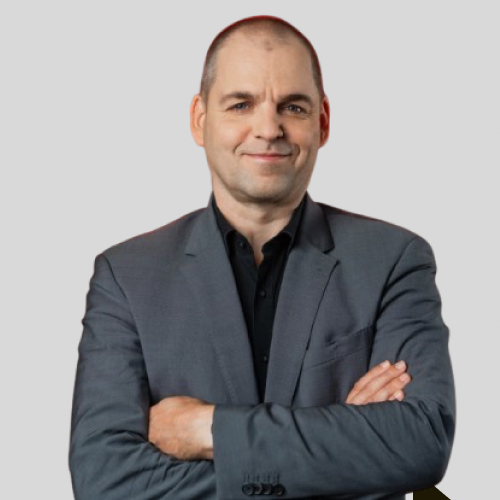
Frank Bösenberg
Silicon Saxony
Frank Bösenberg is the Managing Director of Silicon Saxony, one of Europe’s largest semiconductor clusters and the current chairman of Silicon Europe.
Based in Dresden, he has steered the organization for over a decade, connecting more than 600 members across industry, research, and government. As Chairman of the Silicon Europe Alliance, Bösenberg leads initiatives to foster innovation and strengthen the European semiconductor ecosystem. Deeply committed to Saxony’s, Germany’s and Europe’s economic growth, he promotes cooperation in microelectronics, smart systems, and digital technologies, helping position the region as a global high-tech leader.
Company Profile
With over 600 members, Silicon Saxony is the largest high-tech network in Saxony, one of the largest ICT clusters in Germany and the largest microelectronics cluster in Europe. Completely self-financed, Silicon Saxony has been connecting manufacturers, suppliers, service providers, colleges/universities, research institutes, public institutions and industry-relevant start-ups in Saxony and beyond since its foundation in 2000.
The thematic focus of the cluster is on the technological trends of the present and future – e.g. artificial intelligence, robotics, automation, Internet of Things, sensor technology, energy efficiency, neuromorphic or edge computing. As a close cooperation partner of the Dresden Smart Systems Hub and the Leipzig Smart Infrastructure Hub, Silicon Saxony also offers direct access to the topics, projects and locations of the Digital Hub Initiative of the Federal Ministry of Economics and Technology.
09:10 – 09:20
Public funding opportunities for the semiconductors industry in the EU
The semiconductors industry is among the highest beneficiaries of public funding in the EU. Grants target R&D activities, first industrial deployment of breakthrough innovations and first of a kind manufacturing facilities. Securing such State aid and EU funding is a highly competitive process which requires a thorough understanding of the numerous opportunities and associated regulations. Based on several use cases, Marc Isabelle’s presentation will provide a valuable first dive into public funding opportunities for the semiconductors industry in the EU.
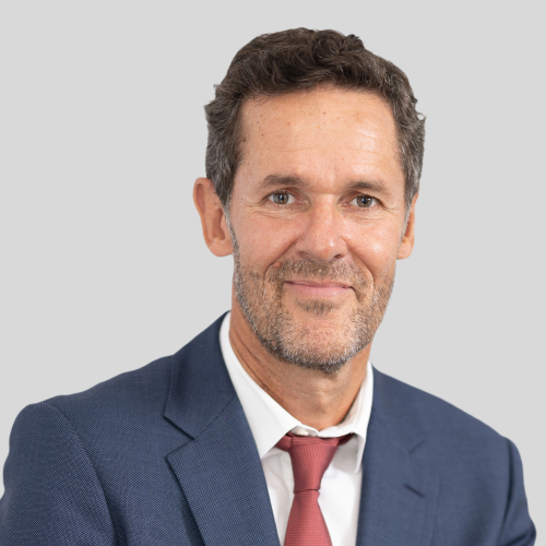
Marc Isabelle, Ph.D.
european economics
Marc ISABELLE, engineer & PhD in Economics, is the founder and CEO of european economics.
Marc is a recognised expert in the public funding of strategic projects. Since 2009, he has helped 195 companies secure €41 billion in public funding for 246 major projects. These initiatives tackle key societal challenges – including disruptive innovation, decarbonisation, resilience and infrastructure – across a wide range of industrial sectors including microelectronics, software, telecoms, automotive, energy and environment, batteries, pharmaceuticals and biotech.
Through his extensive work with the European Commission and national authorities, Marc has actively contributed to shaping the methodologies and best practices used to assess public funding applications and their compatibility with EU regulations.
Company Profile
Founded in 2009, european economics is a recognised pure-player consultancy specialising in public funding. We deliver tailored, high value-added services across Europe to support our clients in designing and implementing turnkey public funding strategies – State aid and European funding – for their most strategic projects:
• €41 billion in public funding secured for 246 projects, including €5.8 billion in 2024,
• 100% success rate for State aid notifications to the European Commission.
Company Products & Services
We support our clients with a turn-key approach at every step of their project’s life-cycle: funding strategy definition, application file preparation (at National and EU level), European Commission validation process, and funding monitoring.
09:25 – 09:45
Keynote
Volkswagen Group Power Electronics Strategy
The presentation will cover our newest power module design, our inhouse prototyping capabilities, and will give an outlook into the future roadmap of our power electronics strategy.
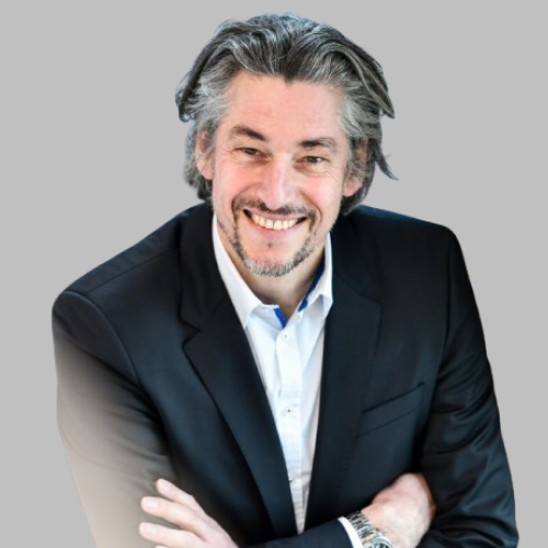
Roman Straßer
Volkswagen Group Technology
Company Profile
As group-wide „Powerhouse“ of Volkswagen, the group resort Technology with its business units is responsible for the core transformation-topics “battery”, “charging and energy”, and “components”. It shapes the development and production of strategic components for the car-manufacturing brands of the group and with its “platform business” also for OEMs outside the Volkswagen Group. As an independent company inside the group resort Technology, Volkswagen Group Components employs 70.000 employees in more than 60 factories worldwide. They provide a valuable contribution for the Volkswagen Group, its brands and products. Thomas Schmall is the board member for the group resort Technology and CEO of Volkswagen Group Components.
09:50 – 10:50
Networking Break, Coffee and Business Meetings
10:55 – 11:15
Keynote
Innovation That Scales: Aligning Semiconductor Breakthroughs with Automotive Value Creation
In today’s automotive landscape, cost pressure is relentless, and the need for fast innovation is evident. As high-voltage technologies rapidly evolve, our challenge is clear: deliver cutting-edge solutions that create tangible value for customers — without compromising on affordability or performance. It is only by aligning chip technology, package concepts, and application understanding that we can ultimately create sustainable value along the automotive value chain.
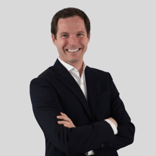
Stefan Obersriebnig
Infineon Technologies AG
Stefan Obersriebnig is Senior Vice President and global business responsible for Infineon Technologies’ automotive module business. During his tenure in various senior-management roles within Infineon, he has had a strong focus on driving the adoption of new Wide-Bandgap devices in the automotive, industrial, and consumer space.
Before joining Infineon, Stefan worked at Siemens Management Consulting in Germany, USA, and lastly as Principal for 3 years in China. He focused on international growth, organizational transformation & cultural change, as well as turnaround & restructuring.
Stefan holds an MBA from IESE Business School (Spain) and a MSc (Honors) in Environmental Engineering from Leoben University (Austria). With his deep connection to nature and the environment, Stefan is passionate about driving Decarbonization & Digitalization for Infineon’s customers.
Company Profile
Here at Infineon, we combine entrepreneurial success with responsible action to make life easier, safer, and greener. Barely visible, semiconductors have become an indispensable part of everyday life. We play a key role in shaping a better future – with microelectronics that link the real and the digital world. Our semiconductors enable efficient energy management, smart mobility, as well as secure, seamless communications in an increasingly connected world. Infineon designs, develops, manufactures and markets a broad range of semiconductors and system solutions. The focus of its activities is on automotive and industrial electronics, communication and information technologies, IoT, sensor technology and security. The product range comprises standard components, software, customer-specific solutions for devices and systems, as well as specific components for digital, analog, and mixed-signal applications.

11:20 – 11:40
Keynote
Power Modules at the Crossroads: Enabling Scalable EV Innovation
Power modules are a key enabler in EV inverter systems—impacting thermal performance, reliability, and serving as the foundation for mechatronic integration. While the efficiency of electric vehicles is primarily driven by semiconductor technology, power modules play a crucial role in realizing that potential at the system level. The market of module manufacturing is highly fragmented, with IDMs, Tier 1s, OSATs, and new entrants each pursuing different business models. This presentation explores how the industry can evolve toward more collaborative and scalable approaches—aligning innovation, integration, and value creation to support the next generation of electric mobility.
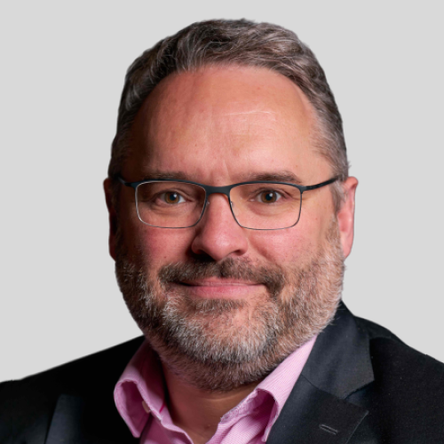
Kai Konrad
Stellantis
Kai Konrad leads Global Semiconductor Purchasing at Stellantis, drawing on over 20 years of experience in the semiconductor and automotive industries. His career spans roles in product and system marketing, innovation management, and supplier relations at companies like Infineon and Renesas. In 2019, he transitioned from marketing to procurement, bringing a strategic and cross-functional perspective to semiconductor sourcing. Passionate about transformation, innovation and collaboration, Kai is committed to shaping resilient, future-ready supply chains that support the evolution of sustainable mobility.
11:45 – 13:30
Buffet Lunch
13:35 – 13:55
Datacenter Trends and Power Architecture evolution
Datacenters are in big disruption with AI proliferation, introducing very fast product cycles. Power consumption at the xPU is increasing dramatically (multi-kW), bringing the total power in the rack up to several hundreds kW to 1MW.
For this reason, conventional architecture of power distribution inside the rack, based on 48V intermediate Bus generated from the AC main, needs to be modified to manage this dramatic increase of power. Current structure of the rack and architecture cannot manage the power increase without incurring in huge distribution losses.
A higher Voltage DC Bus is getting introduced by the Hyperscalers, and supported in R&D by the OEMs and PSU suppliers. This will be generated in an external side-car rack starting from the main AC, while the computational rack will be supplied by this voltage and will contain all the GPUs, or TPUS required to increase the computational performance of the AI infrastructure. The new isolated topologies involved in this high Voltage DC Architecture will require many high voltage switches, especially GaN will be extremely useful, since of the capability to switch extremely fast, and as a consequence enable a smaller size and high power density required by the huge power level of these new Racks. On the low voltage side to generate the intermediate 48V to reuse the existing ecosystem, both Silicon MOSFETs or GaN HEMT can be alternatives to achieve the performance and size requirement.
Other challenges have to be resolved also at lower voltage, where the current required by the GPU will also increase, with values that trend to a few kW. This requires to deliver the power to the load in unconventional ways, with vertical delivery, from the opposite side of the SoC, in the aim to reduce distribution losses. This vertical power delivery (VPD) can be implemented by discrete solutions, or more integrated modular approaches to reduce size and parasitics, integrating inductors and capacitors together with active elements. Renesas is able to supports all these new architectural elements, leveraging its GaN and Si switches portfolio, together with digital controllers for IBC and Multiphase, drivers, and digital and analog PoL and BMS controllers.
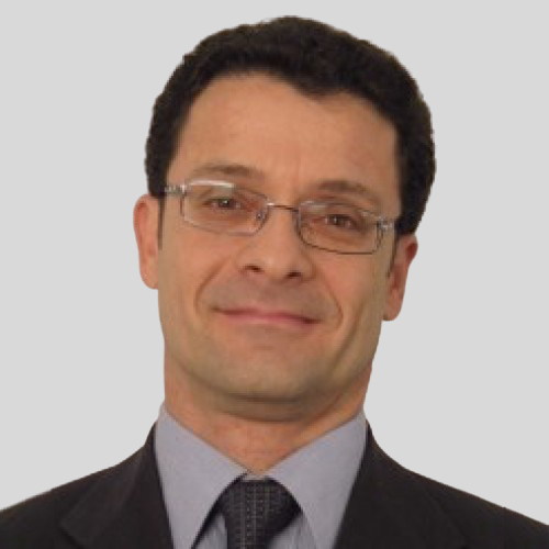
Pietro Scalia
Renesas Electronics Corporation
Pietro Scalia is the Head of System Application and Marketing for Power at Renesas Electronics. His team localized in the three regions is defining and supporting power system solutions for all the market segments, leveraging the entire Power portfolio and addressing new market trends and power architectures.
At onsemi (2021-2023) he lead the Munich Application and PLM team of Automotive EV-Traction Solutions, to define and develop SiC and Si Power Module and Bare DIE portfolio. Previously he worked 11 years at TI, with worldwide Business Development responsibilities on Power products with application focus swinging from Automotive market sector to Telecommunications and Cloud, leveraging his earlier career in Siemens, Ericsson, ST Microelectronics and Academia.
Company Profile
Renesas Electronics empowers a safer, smarter and more sustainable future where technology helps make our lives easier.
A leading global provider of microcontrollers, Renesas combines our expertise in embedded processing, analog, power and connectivity to deliver complete semiconductor solutions. These Winning Combinations accelerate time to market for automotive, industrial, infrastructure and IoT applications, enabling billions of connected, intelligent devices that enhance the way people work and live.

14:00 – 14:20
Advanced low inductance SiC Power Module with 3D wiring technology
An advanced 3D Wiring technology has been developed to increase the power density of modules equipped with silicon carbide (SiC) for electric vehicle (xEV). Applying the multi layer 3D wiring technology with copper pin-terminals demonstrates about twice the power density of a conventional copper clipped wiring structure. The ⊿Tvj power cycling lifetime of power modules with the developed 3D wiring technology is approximately five times longer than the conventional copper clipped wiring.
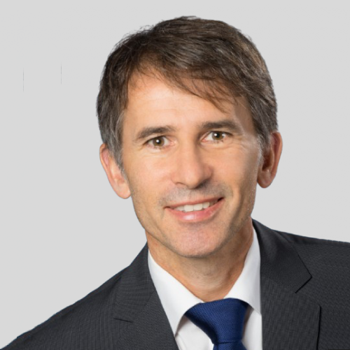
Thomas Heinzel
Fuji Electric Europe
1988 Graduation in Electrical Engineering at DHBW Mannheim
1988-1998 ABB, Mannheim (Traction Division)
• Development of a control unit for a 3-level 3-phase Inverter including the control pattern and PLD algorithm.
• Development and commissioning of a 60 kVA 3-level-Transistor-Inverter for Light Rail Vehicles
• Conception and development of a new Auxiliary Inverter System for Railways
• Project Management of the Auxiliary Inverters at Adtranz, Mannheim
1998 : Fuji Electric Europe GmbH
• Start an Application support for the all Power Semiconductor Customers in the EMEA Sales area
• Build a technical support Team including quality analysis function
• Manager of the technical Department of the Semiconductor Division
• Implementation of a R&D team for EU customers
Since Dec 2021 :
• Head of Semiconductor Technical Division
Company Profile
Fuji Electric specializes in electrical and thermal power engineering, delivering innovative solutions that promote sustainability and energy efficiency. We help customers significantly reduce energy consumption and minimize their carbon footprint with environmentally responsible technologies.
Since 1987, Fuji Electric Europe has been a trusted partner across Europe, the Middle East, and Africa. We’re proud to be a leader in high-performance power semiconductors for automotive and industrial applications. Our extensive product range includes MOSFET devices, diodes, and power semiconductor modules for energy-saving electronics, along with control ICs for high-efficiency power supplies. This ensures we provide reliable, customized solutions for energy-intensive industries, contributing to a more sustainable future.
Company Products & Services
For years, our power semiconductors powered electric drives (like frequency converters and servo drives) and uninterruptible power supplies (UPS). This built our reputation for outstanding quality, high reliability, and cutting-edge technology.
Today, our application portfolio is rapidly expanding into exciting new areas: renewable energy (wind and solar), hybrid/electric vehicles, smart grids for energy supply, and traction systems. Each new application demands innovative, efficient, and durable solutions of the highest quality.
Our state-of-the-art production facilities across front-end, back-end, and warehousing ensure we can supply our growing global customer base with power semiconductors. This guarantees flexible product availability and an excellent price-performance ratio.
Our latest 7th IGBT generation (X series) is now rolling out, seamlessly replacing older products. These new devices offer both electrical and mechanical compatibility while significantly reducing losses, pushing the boundaries of efficiency.
14:25 – 14:45
High-tech HV IGBT and SiC Modules Designed for Railway Applications
Joint Collaboration Presentation
An example of vertical solution implementation through partnership is described in this presentation using rail applications. ŠKODA ELECTRIC and HITACHI ENERGY collaborate on applying high-voltage IGBT semiconductors in various module platforms, including newest LinPak IGBT modules for serial usage in traction converters with a 3 kV DC power supply system. In recent years, the ŠKODA GROUP has been intensively developing hybrid dual-system trains with battery drive for a range of 80-120 km on non-electrified lines. A necessary condition for BEMU is the development of a high-tech DC-DC converter with galvanic isolation of 10 kV and a continuous power of 800 kW. Given the weight of LTO batteries, emphasis was placed on minimum weight and installation dimensions and high efficiency of the converter. This clearly leads to the choice to adopt on power semiconductor side SiC technology both on the 800 V traction battery side and on the 3 kV DC traction converter side. Therefore, the partnership with Hitachi Energy was used to develop a SiC module for a voltage of 3.3 kV with an insulation voltage of 10.2 kV. The development of this semiconductor took place in parallel with the development at ŠKODA ELECTRIC converter development over the last couple of years, leading to the stage that as of today 4 BEMU trains are in operation on Czech Railways and these SiC based semiconductors work absolutely reliably, and were the key enabler for this new train platform. As a further step into performance of this train platform, based on the experience with another SiC Powermodule, the RoadPak SiC, for electric buses, there is now the development of a traction inverter for BEMU trains with these SiC modules with parameters of 1200V and the record current of 1150A for powering asynchronous traction motors with a continuous power of 340 kW. The development of power SiC modules and their application in railways allows to come up with ecological solutions for modern trains and significantly reduce the environmental burden and increase the comfort of passengers on the railway. European cooperation between two major companies is a best practice example of this.
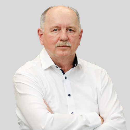
Ladislav Sobotka, Ph.D.
Skoda Electric
Ladislav is the Director of Development and Engineering at ŠKODA ELECTRIC, part of the ŠKODA Group. He joined Skoda in 1982 to develop electric locomotives, where he worked on traction drives. In 1996 he developed a new traction drive for the City Elephant double-decker unit (3 kV DC supply system ) with new HV IGBT transistors and a double star asynchronous traction motor. He also worked extensively on the development of trams and subway vehicles. He has been in the management of ŠKODA TRANSPORTATION since 1994, and in the following years he served as Technical Director and member of the Supervisory Board of ŠKODA TRANSPORTATION. In 2003, he founded ŠKODA ELECTRIC and was a member of the Board of Directors in charge of the technical departments. At ŠKODA ELECTRIC, he has been involved in a number of foreign projects, such as a traction drive for locomotives for Turkey in cooperation with the Korean company Hyundai-Rotem and a groundbreaking traction drive for a subway train for the Chinese city of Suzhou. Ladislav works very intensively with universities and is a member of three scientific councils. Since 2015 he has been working on SiC semiconductors and high efficiency traction drives.
Company Profile
We are Škoda Electric, belonging to the Škoda Group. We continue in the tradition of the one hundred and sixty-year tradition of Škoda plants and we are an experienced manufacturer of traction drives and motors for locomotives, trams, EMU, metro, mining vehicles.

Rainer Kaesmaier, Ph.D.
Hitachi Energy Ltd.
Dr. Rainer Kaesmaier is leading the semiconductor business of Hitachi Energy with its global manufacturing and R&D footprint for the power semiconductor product portfolio which compromises GTOs, IGBTs, IGCTs, Thyristors, Diodes and SiC for market segments such as energy transmission & distribution, transportation & rail, renewables, industry and eMobility. Rainer is a semiconductor industry veteran having held various management and executive positions in the sector for close to 30 years, covering areas of global responsibility in business strategy and development, business transformation, technology and engineering, operations and production, R&D, as well as sales and marketing. After stations at Siemens, Infineon, Qimonda, and the European semiconductor manufacturer LFoundry, he assumed 2018 the responsibility for the global semiconductor business of Hitachi Energy. In addition to that, Rainer is since 2019 also member of the management board for Hitachi Energy Switzerland. He was a member in various industries strategy committees in Europe and the US, and currently in the advisory board for International Semiconductor Industry Group (I.S.I.G.). Rainer holds a Master’s degree in Physics from the Technical University Munich and a PhD in Physics from the University Kassel in Germany. He is based in Lenzburg near Zurich, Switzerland.
Company Profile
We have one of the most diverse semiconductor portfolios that includes thyristors, diodes, GTOs, IGCTs, IGBTs and RoadPakTM modules, which are manufactured at our facilities in Lenzburg, Switzerland and Prague, Czech Republic. We have one of the most diverse semiconductor portfolios that includes thyristors, diodes, GTOs, IGCTs, MOSFETs and IGBTs, which are manufactured at our facilities in Lenzburg, Switzerland and Prague, Czech Republic. Our research team continues pushing the boundaries of what is possible, using silicon and silicon carbide (SiC) technology to innovate the next generation of power electronics devices. Our advanced semiconductor technology brings unprecedented control to HVDC transmission systems. We are the heart of traction converters for high speed trains, metros and diesel-electric locomotives. Pumps, fans, roller tables, hoist and winches found throughout industry rely on us, and the world is able to enjoy greener mobility because we power the next generation of e-vehicles.

14:50 – 16:05
Networking Break, Coffee & Business Meetings
16:10 – 17:10
Panel Session: Electrification Market & WBG Adoption

Moderator
Aly Mashaly
Verotera
Aly Mashaly is the Founder and CEO of Verotera, a German company pioneering next-generation power semiconductor technologies. With over 20 years of experience in power electronics, Aly is a renowned expert in power electronic systems and semiconductors. He holds several patents in the field and is a keynote speaker at numerous international conferences.
Aly earned his degree in Electrical Engineering with a focus on Power Electronics from Ain Shams University in Cairo and moved to Germany in 2002 to pursue his master’s degree at the University of Hanover.
He began his career pioneering the development of power electronic systems for avionic applications before focusing on advancing power electronics for electric mobility. In his most recent role as Technical Director at ROHM Semiconductor Europe, he played a key role in driving the company’s vision to become a global leader in power devices and contributed to growing the business through multi-billion-dollar projects.
Company Profile
Verotera is a German startup and a next-generation semiconductor company driven by deep system-level expertise and a vision for a smarter, cleaner world. Our team brings hands-on experience in inverter development, semiconductor design, and real-world system integration. We operate across the full stack — from chip physics to complete systems — designing technologies that address the actual needs and constraints of modern applications.
This unique positioning allows us to reduce integration costs, accelerate design cycles, and deliver higher system efficiency. With strong industry networks and credibility in both the OEM and semiconductor domains, we bridge the gap between demand and innovation — enabling faster validation, strategic partnerships, and more effective go-to- market execution.
Please visit Verotera’s website for more information: www.verotera.com

Panelist
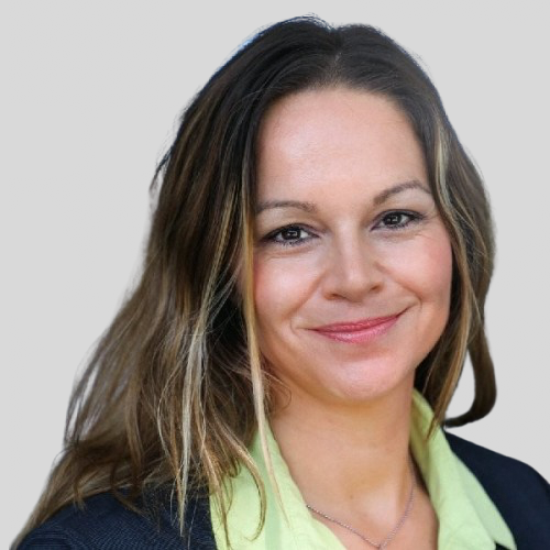
Maike Mueller, Ph.D.
Volkswagen Group Technology
Dr. Maike Mueller graduated in chemistry from Technical University of Munich and received her doctorate from the Humboldt University of Berlin while working at the Federal Institute for Materials Research and Testing. She started her career in the semiconductor industry as a quality and process engineer at Osram Opto Semiconductors in Regensburg. The past 11 years she has been working in various management roles within Infineon’s automotive and consumer divisions as well as procurement department. Since Oct 2024 she joined VW Group as Head of Semiconductor Strategy & Development of Power modules, Group Powerelectronics.
Company Profile
As group-wide „Powerhouse“ of Volkswagen, the group resort Technology with its business units is responsible for the core transformation-topics “battery”, “charging and energy”, and “components”. It shapes the development and production of strategic components for the car-manufacturing brands of the group and with its “platform business” also for OEMs outside the Volkswagen Group. As an independent company inside the group resort Technology, Volkswagen Group Components employs 70.000 employees in more than 60 factories worldwide. They provide a valuable contribution for the Volkswagen Group, its brands and products. Thomas Schmall is the board member for the group resort Technology and CEO of Volkswagen Group Components.


Panelist
Ralf Bornefeld
Bosch
Ralf Bornefeld is Senior Vice President with responsibility for the business unit Power Semiconductors & Modules at Bosch.
Before he held various management positions at Infineon Technologies AG: senior director technology in frontend production from 2005-2008, senior director engineering of automotive sensors until 2011 and finally vice president and general manager business line automotive sensors.
Ralf started his career at Elmos Semiconductor in 1992 as a technology development engineer. Afterwards he took several management positions until end of 2004, mostly serving as vice president of R&D and eventually as vice president of business line microsystems.
Ralf Bornefeld was born in Schalksmuehle, Germany, in 1964. He graduated with a degree in Electrical Engineering from Technical University of Dortmund in 1992.
Company Profile
The Bosch Group is a leading global supplier of technology and services. It employs roughly 428,000 associates worldwide (as of December 31, 2023). According to preliminary figures, the company generated sales of 91.6 billion euros in 2023. Its operations are divided into four business sectors: Mobility, Industrial Technology, Consumer Goods, and Energy and Building Technology. As a leading IoT provider, Bosch offers innovative solutions for smart homes, Industry 4.0, and connected mobility. Bosch is pursuing a vision of mobility that is sustainable, safe, and exciting. It uses its expertise in sensor technology, software, and services, as well as its own IoT cloud, to offer its customers connected, cross-domain solutions from a single source. The Bosch Group’s strategic objective is to facilitate connected living with products and solutions that either contain artificial intelligence (AI) or have been developed or manufactured with its help. Bosch improves quality of life worldwide with products and services that are innovative and spark enthusiasm. In short, Bosch creates technology that is “Invented for life.” The Bosch Group comprises Robert Bosch GmbH and its roughly 470 subsidiary and regional companies in over 60 countries. Including sales and service partners, Bosch’s global manufacturing, engineering, and sales network covers nearly every country in the world. The basis for the company’s future growth is its innovative strength. At 136 locations across the globe, Bosch employs some 90,000 associates in research and development, of which roughly 48,000 are software engineers.

Panelist
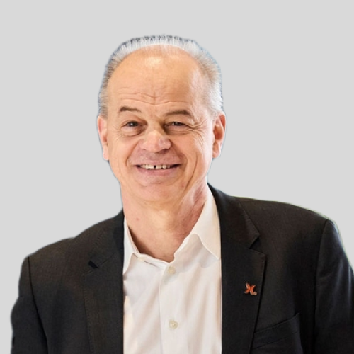
Edoardo Merli
Nexperia
Edoardo Merli, SVP and GM of Business Group Wide Band Gap, IGBT & Modules, is a highly accomplished executive with 30+ years in high-tech and automotive industries.
He brings a solid experience on semiconductors, both in automotive and industrial/consumer domains.
Before joining Nexperia, he was EVP and GM of Power Transistor SubGroup in STMicroelectronics.
His previous assignments included automotive processors and infotainment, communications, RF and -the latest one- Power Technologies.
Edoardo holds a BA in Engineering (B. Eng.), Electrical, Electronics and Communications Engineering from University of Bologna in Italy.
Company Profile
Headquartered in the Netherlands, Nexperia is a global semiconductor company with a rich European history and over 15,000 employees across Europe, Asia, and the United States. As a leading expert in the development and production of essential semiconductors, Nexperia’s components enable the basic functionality of virtually every electronic design in the world – from automotive and industrial to mobile and consumer applications.
The company serves a global customer base, shipping more than 100 billion products annually. These products are recognized as benchmarks in efficiency – in process, size, power, and performance. Nexperia’s commitment to innovation, efficiency and stringent industry requirements are evident in its extensive IP portfolio, its expanding product range, and its certification to IATF 16949, ISO 9001, ISO 14001 and ISO 45001 standards.

Panelist
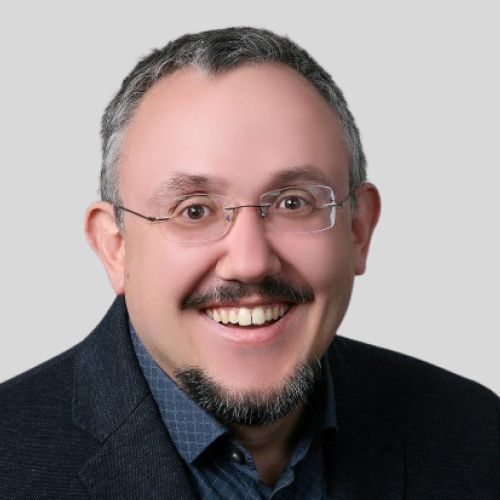
Patrick Schwarz, Ph.D.
Huawei Technologies Co., Ltd.
Patrick Schwarz has studied chemistry in Regensburg, Germany where he completed his PhD in inorganic chemistry. He joined Infineon in 2011 as an engineer for reliability and analytics focusing on chip embedding technologies. 2013 he transferred from RnD to production in the area of process integration and transfer management , where he also took his first management role in 2015 as head of process integration and product engineering for laminate based packages. With the start of Infineons first molded power module Hybridpack DSC he took leadership of the ramp up management for the new platform becoming a specialist for critical new product introductions. After shifting to global productivity platform owner for preassembly within Infineon he joined Huawei as Lab Director for Power Packages in 2024.
Company Profile
Founded in 1987, Huawei is a leading global provider of information and communications technology (ICT) infrastructure and smart devices. We have approximately 208,000 employees and we operate in over 170 countries and regions, serving more than three billion people around the world. We are committed to bringing digital to every person, home and organization for a fully connected, intelligent world.
At Huawei, we have two key drivers of innovation: science and technology, and customer needs. Both commercial value and market demands are driving our innovation and determining how we invest in science and technology. Breakthroughs in technology, in return, stimulate customer needs and allow us to create greater value for customers.
In 2024, our total R&D spending reached CNY179.7 billion, representing 20.8% of our total revenue.
Our total R&D investment over the last decade now exceeds CNY1.249 trillion.
On December 31, 2024, 113,000 employees (about 54.1% of our workforce) worked in R&D.
Through years of sustained innovation in fundamental domains, Huawei has become one of the world’s largest patent holders, currently holding 150,000+.

Panelist
Kai Konrad
Stellantis
Kai Konrad leads Global Semiconductor Purchasing at Stellantis, drawing on over 20 years of experience in the semiconductor and automotive industries. His career spans roles in product and system marketing, innovation management, and supplier relations at companies like Infineon and Renesas. In 2019, he transitioned from marketing to procurement, bringing a strategic and cross-functional perspective to semiconductor sourcing. Passionate about transformation, innovation and collaboration, Kai is committed to shaping resilient, future-ready supply chains that support the evolution of sustainable mobility.

Panelist
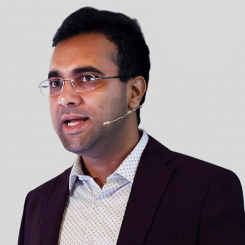
Ajay Poonjal Pai, Ph.D.
Sanan Semiconductor
Dr.-Ing. Ajay Poonjal Pai obtained his B. Tech in Electrical & Electronics Engineering from NITK Surathkal, India and M.Sc. in Electrical Power Engineering from RWTH Aachen University, Germany. He then pursued his PhD focusing on Silicon Carbide (SiC) power semiconductors for automotive traction inverter applications at the Friedrich Alexander University (FAU), Erlangen-Nuremberg, Germany. From 2015 to 2023, he worked at Infineon Technologies AG, Germany as a Principal Engineer responsible for next-generation automotive SiC technologies and power modules. Since May 2023, he is working at Sanan Semiconductor Munich, where he is responsible for building and growing the Wide Bandgap (WBG) Innovation and Application engineering organization. His research interests include e-mobility, SiC semiconductors, power modules and power electronics, and has contributed to numerous invited lectures and conferences worldwide.
Sanan Semiconductor is a wholly-owned subsidiary of the listed company Sanan Optoelectronics. Sanan is committed to becoming a world-class R & D, manufacturing and service platform for wide bandgap semiconductors. Sanan Semiconductor extended Sanan Optoelectronics’ 20-year compound semiconductor industrialization experience to the field of power electronics, and became a full-chain integration platform focusing on the wide bandgap semiconductor industry and providing the most comprehensive products and services.
Panelist
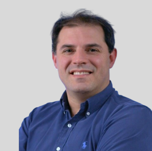
Denis Marcon, Ph.D.
Innoscience
Denis Marcon received a M.S. degree from the University of Padova in 2006. Subsequently, he received the degree of Doctor in Engineering (Ph. D.) from the Catholic University of Leuven and imec with the thesis entitled “Reliability study of power gallium nitride based transistors” in 2011. He is leading author or co-author of more than 50 journal papers or international conference contributions.
After his Ph.D. graduation, he has been leading projects aiming to develop GaN HEMTs for several applications (RF and power switching). Thereafter, he has joined the business development team of Imec where he was directly responsible for the partnerships with imec in the field of GaN power electronics as well as on dedicated development and manufacturing of Si-based devices, MEMS, sensors and micro-systems,
Today he is the General Manager of Innoscience Europe (subsidiary of Innoscience) and he is directly responsible for Innoscience’s GaN business in Europe.
Innoscience (HKEX:02577.HK) is the global leader in gallium nitride process innovation and power device manufacturing. Innoscience’s device design and performance set the worldwide standard for GaN, and the culture of continuous improvement will accelerate GaN performance and market adoption. The company’s gallium nitride products are used in multiple low, medium and high voltage applications, with GaN process nodes covering 15V to 1200V. Wafers, discrete devices, integrated power ICs, and modules provide customers with robust GaN solutions. With 800 patents granted or pending, Innoscience’s products are known for reliability, performance, and functionality within the fields of consumer electronics, automotive electronics, data centers, renewable energy and industrial power. Innoscience creates a bright future for GaN. Please visit www.innoscience.com for more information.

17:15 – 17:25
Enabling Solutions for GaN Processing
Gallium Nitride (GaN) is one of the most important third generation semiconductor materials. Its wide bandgap makes it an excellent candidate for power electronics – GaN high electron mobility transistors (HEMTs) have already become well established in Specialty Technology applications such as consumer fast charging and are gaining traction in automotive. In addition, GaN and its compounds are gaining momentum across a wider range of applications, including µLEDs and RF power amplifiers.
Whilst the properties of GaN bring exciting benefits to these applications it also poses some unique processing challenges. Lam has led the advancement of process technologies for 200 mm GaN on Si fabrication for almost a decade and is also enabling the transition to 300 mm GaN on Si device manufacturing.
In this paper, we will discuss some critical challenges and solutions for GaN processing both, on 200mm and 300mm Si substrates.
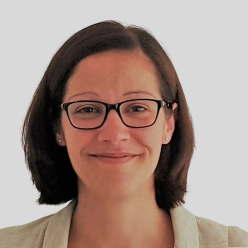
Annika Peter
Lam Research Corporation
Annika joined Lam Research in 2017 and is currently Senior Technology Manager responsible for the Specialty Technologies application space. She previously held positions in engineering and program management, where she was partnering with our customers to enable future device generations. Holding her first fully processed device wafer in 2007, Annika received a B.Eng. in Mechatronics and Microsystems in 2008 and a M.Sc. in Applied Physics in 2011. In 2009 Annika joined a research group at the Institute of Micro Technologies, developing waveguides with integrated optics for bio-sensing. Prior to joining Lam Research Annika was part of the Technology Group at Oxford Instruments Plasma Technology, where she led multiple equipment and process developments.
Company Profile
Lam Research Corporation is a trusted global supplier of innovative wafer fabrication equipment and services to the semiconductor industry. Our strong values-based culture fuels our progress, and it’s through collaboration, precision, and delivery that we are driving semiconductor breakthroughs that define the next generation. Lam Research (Nasdaq: LRCX) is a FORTUNE 500® company headquartered in Fremont, California, with operations around the globe. Learn more at www.lamresearch.com
Company Products & Services
We combine superior systems engineering, technology leadership, and a commitment to customer success to advance the global semiconductor industry. Our broad portfolio of market-leading deposition, etch, strip, and wafer cleaning solutions helps customers achieve success on the wafer by enabling device features that are 1,000 times smaller than a grain of sand—it’s why nearly every chip today is built with Lam technology.

17:30 – 17:40
Wet Process Technology Roadmap for Power Device Manufacturing
In this work we demonstrate strain relief etching using an advanced chemical etching (ACE) process of the full wafer surface on commercial grade n-type 4H-SiC at production throughputs (μm’s/hr). The data shows >4x improvement of breakage strength in laser split wafers. Warp and bow of ground wafers is reduced to match wafers that have been CMP processed showing the potential of stronger, flatter wafers being available for chemical mechanical polishing.
Strain relief etching is a critical wet process technique use in high volume manufacturing of semiconductor substrates and device wafers. The goal of a strain relief etch is application dependent but can generally be considered for removal of warp/bow or improving mechanical strength by removing sub-surface damage thereby optimizing yields. Silicon Carbide (SiC) has a high chemical resistance which has blocked the manufacturing community from using strain relief etching to date.
Without an effective wet etch, the SiC substrate manufacturing community has resorted to expensive mechanical techniques for the polishing and thinning of wafers, which imparts significant stress and strain within the layer. Use of extensive mechanical techniques is also expensive and difficult to perform at volume where wafers are fragile early in the substrate manufacturing line. Research has explored mechanisms of wet etching for creating microstructures on 4H-SiC and trenches in 6H-SiC.
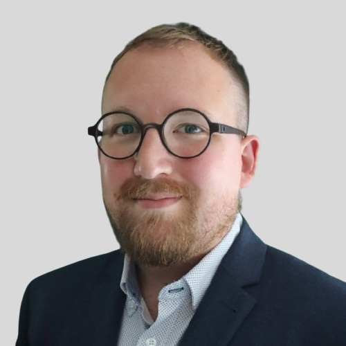
Oliver Whear
RENA Technologies
Oliver Whear is an 11 year industry veteran working at several points in FEOL manufacturing on metrology, deposition and wet process. He started as an applications scientist before moving in to project management and his current role as Director of Semiconductor Technology at RENA Technologies. Oliver is an expert at developing new manufacturing technologies based on challenges foreseen by industrial roadmaps and market strategy.
Company Profile
Founded in 1993, RENA Technologies has established itself as a global leader in mechanical and process engineering, for a diverse range of industries. We specialize in providing cutting-edge wet processing solutions for the semiconductor, solar, additive manufacturing, glass, and medtech industries.
A key area of expertise is wet chemical immersion, spray and single wafer processes for the manufacturing of semiconductors. With over 1,100 systems installed worldwide, our technology is trusted by manufacturers around the globe to enhance efficiency and production quality.
RENA Technologies employs approximately 1,000 professionals worldwide, all dedicated to innovation and excellence in our field. Headquartered in Gütenbach, Germany, and manufacturing sites in Albany, OR and Wykroty, Poland, we continue to drive advancements in process engineering, ensuring our customers receive the highest quality solutions for their manufacturing needs.
On top we provide worldwide onsite service support with over 150 Experts in 20 locations globally to ensure flawless installation and operation of our tools.
Company Products & Services
RENA products are used in path-breaking application fields such as semiconductors, MedTech, renewable energies, the glass industry and additive manufacturing. RENA equipment is used to treat or modify surfaces of, for example, semiconductor wafers, solar cells, glass, optical substrates, 3D-printed metal components or other high-tech products using wet chemical processes like etching, stripping, cleaning or drying. RENA offers proven standard machines as well as customer-specific solutions and process support.

17:45 – 18:00
Networking Transfer and Walk
18:00 – 18:30
Boarding
18:30 Cruise Departure
18:30 – 19:30
Cocktail Reception
19:30 – 21:30
Gala Dinner
Awards Ceremony
Dr. John Palmour Excellence Award
End of content
End of content