9-11 December 2025
Muscat, Oman
No posts
27-28 August 2025 - Suwon


09:00 – 09:35
Registration
09:40 – 10:00
Welcome Speech

Salah Nasri
International Semiconductor Industry Group (ISIG)
Salah Nasri is the CEO and Co-Founder of the International Semiconductor Industry Group (ISIG), a global organization founded in 2010 that connects and empowers semiconductor decision-makers through strategic leadership platforms, executive summits, and collaborative initiatives. ISIG has become a trusted global hub for industry leaders driving innovation and progress across the semiconductor value chain.
With extensive experience across the semiconductor sector, Salah has played a pivotal role in fostering global collaboration among industry leaders. Under his leadership, ISIG has evolved into one of the most influential communities in the semiconductor ecosystem—bringing together executives, innovators, and policymakers across regions including the United States, Europe, Asia, and the Middle East.
Salah has been instrumental in expanding ISIG’s reach and impact, curating high-level summits and initiatives that drive dialogue and progress across critical areas such as semiconductor manufacturing, AI, MEMS, automotive electronics, and advanced packaging. His vision continues to position ISIG as a key platform for thought leadership, networking, and strategic industry alignment.
Earlier in his career, Salah held positions at Credit Suisse, Goldman Sachs, Worldwide Business Research, and the International Business Development Group. He studied International Relations and Economics at Oxford University and Loughborough University, and in 2024 became a Stanford University alumnus after completing the Stanford Executive Program. In addition to his role at ISIG, Salah also serves on the Advisory Board of Atlant3D, a pioneer in atomic-layer advanced manufacturing solutions.
Company Profile
Established in 2010, the International SemiconductorIndustry (I.S.I.G.) is a prestigious & trusted associationwithin the semiconductor industry, renowned fororchestrating major regional summits across the globe,ranging from the U.S, the Middle East & Asia via ourdivision, the International Semiconductor ExecutiveSummits (I.S.E.S.). Our summits are fully endorsed bylocal governments and leading companies in all areas ofthe semiconductor supply chain.
Moreover, I.S.E.S. serves as the Premier platform for senior executives in technology, manufacturing, and R&D from diverse semiconductor companies, technology providers, and affiliated industries.
Our events are instrumental helping to shed light onto key industry trends, drive innovation and influence key decisions to help shape, and advance the growth of the semiconductor sector.

Joshua Yoo
Core Insight, Inc.
Yong Hoon (Joshua) Yoo has been involved in the static control industry since 1994 for ionization, ESD measurement and high voltage power business operation in semiconductor, flat panel displays and automotive industry. He has been a member of EOS/ESD Association since 2000 and served as an Elected Board of Director in 2016 – 2018. He is the founder and president of Korea EOS/ESD Association since 2011. He is a member of Institute of Electronics and Information Engineers (Korean IEEE) since 2021. He is serving industry as Korea President of International Semiconductor Executive Summits (ISES) since 2024.
He started his volunteering activities on EOS/ESD Association since 2013 as an active working group members and technical program committee members of annual symposium for multiple events of ESD Association. With his leadership, Korea EOS/ESD Association very strongly presents and annual events over 10 years. He is pioneer for flat panel display (FPD) static issue analysis and resolved problems. In recently, he found a root cause of ESD yield losses in AI chip manufacturing environment and improved yield over double digits.
He is an iNARTE certified ESD Engineer in 2007 and the EOS/ESD Association certified Professional ESD Program Manager in 2011. He has 14 patents for ionization system and ESD testing technologies.
Company Profile
Core Insight is a leading company for EOS/ESD control with technical expertise and key insights for Advanced Package Device application. Heterogeneous Integration technology revolutionary achieved new device era. This new technology also brought new challenges that much less ESD sensitivity before it finished package device. Core Insight has prepared to meet new level of ESD control with world best ionization solution which no one else have. Core Insight has understanding device technology, manufacturing process and ESD control know-how for Advanced Package Device handling.

10:00 – 10:20
Keynote
HBM Technology and Challenges
Major semiconductor players accelerate the competition to lead semiconductor industry hegemony by the evolution of advanced packaging technology such as chiplets and 2.5D/3D heterogeneous integration. By the evolution of advanced packaging technologies, SK hynix will continuously lead the competitiveness of memory business and prepare the business innovation for beyond memory era.

Kangwook Lee, Ph.D.
SK Hynix
Dr. Lee has been one of critical leaders who are leading the era of 3D TSV stack memory such as HBM (High Bandwidth Memory) in semiconductor industry.
He has contributed broadly to, and led teams in, 3D integration/packaging R&D including core technology/product development/reliability study and mass production for HBM over 27 years.
Dr. Lee received the Ph.D. degree in machine intelligence and systems engineering from Tohoku University, Japan, in 2000. During his doctoral research at Tohoku University,Dr. Lee proposed a new 3D-IC integration technology to achieve 3D devices with high performance and multi-functionality, leading this field in the world.
From 2001 to 2002, he was a Postdoctoral Researcher with the Department of Electrical, Computer, and Systems Engineering, Rensselaer Polytechnic Institute, Troy, NY, USA.
He worked with Memory Division, Samsung Electronics Ltd., Korea, as a Principal Engineer from 2002 to 2008.
From 2008 to 2016, he worked with the New Industry Creation Hatchery Center (NICHe), Tohoku University, Japan, as a Professor.
From 2017 to 2018, he worked with R&D center, Amkor Technology Korea, as a VP.
He joined SK hynix 2018 and currently Senior VP, Head of PKG Development at SK Hynix, Korea.
Dr. Lee has led many interdisciplinary R&D programs on 3D integration, including integration of various materials and devices to achieve 3D devices/systems with high performance and new functionality, 3D-IC reliability research to investigate the impacts of 3D integration on the device performance and reliability, unique hybrid integration of nano-materials with Si, and product development of 3D stack DRAM such as high-bandwidth memory (HBM). For over 27 years at universities and industries in Japan, US, and Korea, Dr. Lee has made exceptional technical contributions to and lasting impacts on 3D integration technology and 3D product development in broad fields, such as material science, materials characterization/analysis, semiconductor device/process, electrical packaging, and Si micro-machining.
Dr. Lee has authored more than 230 scientific publications (peered journals, international conferences), co-edited 4 books, and given 43 tutorial/invited/keynote talks in international conferences including IEEE IEDM, IEEE IRPS, VLSI Symposium, plus 23 US patent publications.
He has served as a frequent reviewer for a number of journals, including IEEE EDL, IEEE T- ED, IEEE CPMT, and technical program committees of international conferences, including IEEE ECTC, IEEE IRPS, IEEE EDTM, IEEE 3D SIC.
He is a Senior Member of IEEE.
Company Profile
An AI First Mover Leading the Global AI Memory Era
With our global technology leadership, SK hynix aims to provide greater value to all stakeholders, including our customers, partner companies, investors, local communities, and employees.
Moreover, we are working to strengthen our ESG management to create even more value, by moving away from the conventional business model of seeking only economic benefits, in pursuit of more social value and a healthier governance structure.
SK hynix will grow into a Full Stack AI Memory Provider, offering customized solutions tailored to the diverse needs of global customers, covering both DRAM and NAND flash, in the era of full-scale AI.

10:20 – 10:40
Keynote
The futrue of Advanced Package for AI application.
As the Moore’s law reach the limitation, Si fabrication process need extremely high cost solutions such as multiple patterning and EUV (Extreme Ultra-Violet) lithography. In spite of high cost Si fabrication process, chip size is increased over the reticle size limit by adding more and more functional blocks for high performance computing. In particular, with the continuous demand for higher performance and capacity in memory products, the amount of data created, processed, stored and transferred is increasing tremendously. In order to overcome these challenges, advanced package has been actively used for heterogeneous integration in electronic packages since the past decade. 2.5D Si interposer architecture has been widely used for horizontal interconnection between logic to logic and logic to high bandwidth memory integration. In this talk, recent advanced package technology and key roadmap in Samsung Electronics will be shared for AI application.
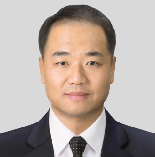
Dae-Woo Kim, Ph.D.
Samsung
Dae-Woo Kim, Corporate VP at Samsung Electronics for 7 years with advanced package technology and product development. In his current position, Dae-Woo is leading the system package lab for product & technology development including 2.xD, 3D, FOWLP and FOPLP technology.
Prior to joining Samsung Electronics, he was a TD Engineering manager at Intel ATTD, Chandler Arizona. During 14 years of experience at Intel, he worked on CPI area, assembly test chip design, Si bridge design and package process & design integration for CPU flip chip package, EMIB, and Foveros technology.
Dr. Kim received a Ph. D., Master and bachelor degree in Material Science Engineering from Yonsei University, Seoul, S. Korea, Country and he was a research faculty in III-V semiconductor field for 3 years at Arizona State University, Tempe, AZ.
Company Profile
Samsung Electronics Co., Ltd. engages in the manufacturing and selling of electronics and computer peripherals. The company operates through following business divisions: Consumer Electronics, Information Technology & Mobile Communications and Device Solutions. The Consumer Electronics business division provides cable television, monitor, printer, air-conditioners, refrigerators, washing machines and medical devices. The Information Technology & Mobile Communications business division offers handheld products, communication systems, computers and digital cameras. The Device Solutions business division comprises of memory, system large scale integrated circuit and foundry. The company was founded on January 13, 1969 and is headquartered in Suwon, South Korea.

10:45 – 11:45
Networking and Coffee Break
Business Meeting Slot 3
11:50 – 12:10
Keynote
Co-Packaged Optics: Powering the Next Generation of Data Center Connectivity for the AI Era
The rapid advancements in machine learning—particularly large language models (LLMs)—are driving an exponential increase in compute demands, with requirements growing by roughly an order of magnitude every 18 months. Traditional gains in silicon scaling are no longer sufficient, prompting a shift from general-purpose computing to accelerated computing and massive parallelism. This evolution amplifies the critical role of interconnect bandwidth, now a primary system bottleneck. Co-packaged optics (CPO) offer a transformative path forward, delivering scalable, high-bandwidth, and energy-efficient interconnects for next-generation workloads. Realizing CPO’s full potential will require advances in 2.5D and 3D integration to achieve new levels of performance and efficiency. In this talk, we will examine the state of current CPO solutions and explore the integration and scaling options that can unlock their full promise.
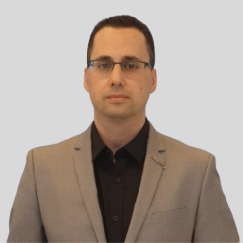
Liron Gantz, Ph.D.
NVIDIA
Dr. Liron Gantz has led Nvidia’s Electro-Optics group (NVEO) for the past six years, driving advancements in silicon photonics for Co-Packaged Optics products. He completed his Ph.D. in 2017. In 2016 he joined Mellanox, where he established the electro-optics lab for device characterization. He quickly transitioned into leadership roles, specializing in the design, characterization, and modeling of silicon photonic technologies. Dr. Gantz and his team have been instrumental in the Nvidia CPO project, from its inception to chip development and system bring-up. Dr. Gantz is now a Principal Research Scientist in Nvidia’s research organization. With a strong foundation in Quantum Mechanics, Nanotechnology, and Optics, he has published in leading journals such as Science and Physical Review Letters, highlighting his contributions to the semiconductor industry.
Company Profile
Since its founding in 1993, NVIDIA (NASDAQ: NVDA) has been a pioneer in accelerated computing. The company’s invention of the GPU in 1999 sparked the growth of the PC gaming market, redefined computer graphics, ignited the era of modern AI and is fueling the creation of the metaverse. NVIDIA is now a full-stack computing company with data-center-scale offerings that are reshaping industry.

12:10 – 12:30
Keynote
Breaking Barriers with Glass: A New Era in Semiconductor Integration
As semiconductor packaging evolves to meet the demands of AI, high-performance computing, and RF systems, traditional organic and silicon-based substrates are nearing their limits. Glass substrates are emerging as a compelling alternative, offering exceptional electrical performance, dimensional stability, and scalability. With ultra-low dielectric loss, fine-pitch interconnect capability, and compatibility with Through-Glass Vias (TGVs), glass enables higher signal integrity and integration density. Its thermal expansion match with silicon also enhances reliability in advanced packages. Despite challenges—such as mechanical fragility, TGV metallization, and thermal management—ongoing innovations in materials and process engineering are rapidly closing the gap. This keynote explores the transformative potential of glass substrates, the hurdles to their widespread adoption, and the collaborative efforts shaping a new ecosystem for next-generation semiconductor packaging.

Sung Jin Kim, Ph.D.
Absolics
Dr. Kim is the CTO of Absolics, a spun-off semiconductor packaging business from SK Group in the USA. With 31 years of experience in the semiconductor and microelectronic packaging industry, Dr. Kim leads new technology and business development for advanced semiconductor packaging solutions at Absolics. Prior to Absolics, he held executive positions in various companies and countries, including SKC, Georgia Institute of Technology, Foxconn Advanced Technology, Daeduck Electronics, UTAC, and Amkor Technology. Throughout his career, Dr. Kim managed package engineering, substrate manufacturing, and embedding component microelectronic package engineering. He has over 200 US patents and holds a doctorate in electrical engineering from the Technical University of Dresden, Germany.
Company Profile
Absolics is a leading provider of advanced packaging technologies and services, offering scalable solutions for businesses of high-performance computing. We offer smart, innovative services to dozens of clients globally.
12:35 – 13:45
Lunch Break
13:50 – 14:10
Advanced Power Packaging for AI Power solution: UTAC’s Thermally Enhanced QFN and 3D Module Solutions for Optimized Efficiency and Integration
Reserved
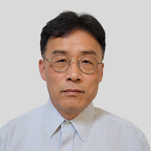
Michael Choi
UTAC Group
Hyungmook Choi is a seasoned semiconductor expert with over 30 years of experience in the power semiconductor industry. He holds B.S. and M.S. degrees in Electrical Engineering from Seoul National University. Starting at Samsung Semiconductor, he advanced through leadership roles at VISHAY SILICONIX and UTAC, where he pioneered QFN copper clip technology and expanded into WBG markets. Under his guidance, UTAC shipped over 3 billion QFNs with copper clips by 2024. Mr. Choi is a respected keynote speaker and is currently focused on AI power QFN and SiP development to meet future industry needs
Company Profile
UTAC Group is a leading outsourced semiconductor assembly and test (OSAT) provider, founded in 1997 and headquartered in Singapore. The company specializes in advanced assembly and test services for logic, memory, analog/mixed-signal, image sensors, MEMS, and power devices. UTAC supports a global customer base that includes fabless companies, integrated device manufacturers (IDMs), and wafer foundries.
With ten manufacturing facilities across Singapore, Thailand, China, and Indonesia, and a robust global sales network spanning North America, Europe, Greater China, Japan, and Southeast Asia, UTAC delivers comprehensive turnkey solutions—from wafer probing to final testing.
UTAC serves diverse market segments including automotive, computing, communications, consumer electronics, and industrial applications. Renowned for its reliability, technological expertise, and customer-centric approach, UTAC continues to play a vital role in enabling next-generation semiconductor innovation.
Company Products & Services
UTAC Group provides a comprehensive range of semiconductor assembly and test services, delivering turnkey solutions from wafer probe to final test across key end markets.
Its packaging portfolio includes leadframe-based packages such as QFN, DFN, QFP, TLA, and Cu-clip variants, as well as laminate-based BGA/iBGA packages for mobile, computing, and automotive applications. UTAC also offers System-in-Package (SiP) modules that integrate multiple components into compact, high-density solutions for IoT, wearables, and automotive electronics.
Advanced wafer-level offerings include bumping services and Wafer-Level Chip Scale Packaging (WLCSP) for customers requiring miniaturization, high electrical performance, and low-profile form factors.
UTAC also supports image sensor packaging, including automotive-grade iBGA with cleanroom assembly to meet stringent reliability and contamination standards.
To complement mass production, UTAC provides value-added services such as package design support, reliability qualification, and failure analysis—helping customers accelerate time to market with confidence.
14:10 – 14:20
Enabling next-gen AI with ASMPT’s Total Interconnect Solutions
ASMPT Semiconductor Solutions stands at the forefront of the AI revolution, delivering comprehensive advanced packaging technologies essential for next-generation artificial intelligence applications. As AI workloads demand exponential increases in interconnect density and performance, ASMPT Semiconductor Solutions’ total interconnect solutions portfolio addresses critical challenges across CoWoS, HBM, and heterogeneous integration. Our pioneering thermo-compression bonding (TCB) technologies, including the industry-first fluxless AOR™ process, enable the precise sub-micron connections required for AI logic processors and high-bandwidth memory integration. With proven capabilities spanning first-level interconnect solutions for HPC and data center applications such as silicon photonics, co-packaged optics, logic, CoWoS and HBM packaging, ASMPT Semiconductor Solutions empowers the Intelligence Revolution, supporting applications from cloud computing to edge AI deployment across automotive, industrial, and telecommunications sectors.
Choon Khoon Lim
ASMPT Semiconductor Solutions
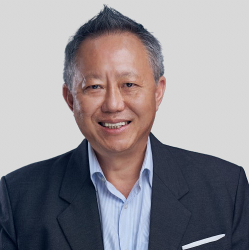
LIM Choon Khoon (CK) is a Senior Vice President and Chief Executive Officer of Semiconductor Solutions Advanced Packaging (AP).
CK’s career spans key engineering, manufacturing, and regional functional and global general management roles with several global semiconductor companies. As Chief Executive Officer of the Segment’s AP Business Group, he helps provide the industry’s leading first-level interconnect technologies covering leading AP First Level Interconnect (FLI) technologies for logic, HBM, Si Photonics & Co-Packaged Optics, wafer die singulation solution for advanced fabricated wafers and Panel ECD for fine Line/Space organic and glass substrate & Wafer PVD, that are well-positioned to serve and to scale with the most demanding AP needs.
CK holds a Bachelor of Science (Honours) in Production Engineering and Production Management degree from the University of Nottingham, United Kingdom
Company Profile
ASMPT Limited, founded in 1975, is headquartered in Singapore and is listed in Hong Kong Stock Exchange since 1989.
ASMPT is the only company in the world that offers high-quality equipment for all major steps in the electronics manufacturing process – from carrier for chip interconnection to chip assembly and packaging to SMT. No other supplier offers a comparable range and depth of process expertise.
Semiconductor Solutions Segment Business of ASMPT offers a diverse product range from bonding to molding and trim & form to the integration of these activities into complete in-line systems for the microelectronics, semiconductor, camera modules, advanced packaging, photonics, and optoelectronics industries.
The group has successfully established itself as the leading player in the back-end assembly and packaging market with its innovative solutions and constant focus on customer value creation.

14:20 – 14:30
Atomic-Scale Manufacturing for Next-Gen Advanced Packaging
Advanced packaging demands ultra-precise material engineering—from hybrid bonding to reliable edge passivation. ATLANT 3D’s patented Direct Atomic Layer Processing (DALP®) technology enables on-demand, localized atomic layer processing of functional materials. Our approach eliminates the need for masks, vacuum chambers, and lithography steps—making it ideal for interface tailoring in advanced packaging. Join us to explore how atomic-scale processing can unlock novel integration schemes, improve device yield, and accelerate lab-to-fab transitions in the era of heterogeneous integration and chiplet architectures.

Maksym Plakhotnyuk, Ph.D.
ATLANT 3D
Dr. Maksym Plakhotnyuk, is the CEO and Founder of ATLANT 3D, a pioneering deep-tech company at the forefront of innovation, developing the world’s most advanced atomic-scale manufacturing platform. Maksym is the inventor of the first-ever atomic layer advanced manufacturing technology, enabling atomic-precision development of materials, devices, and microsystems. A scientist with a Ph.D. in Nanotechnology, he has deep expertise in nanotechnologies, renewable and exponential technologies, semiconductor processing, solid-state physics, and material science. A Fulbright scholar, Hello Tomorrow Grand Winner, and proud Ukrainian, Maksym has earned global recognition for his work.
Company Profile
ATLANT 3D has mastered control of matter at the atomic scale, ushering in a new era in manufacturing. For research teams and manufacturers working at the frontiers of technology, we’ve created what was once thought unattainable: a system that builds materials and devices, atom by atom, with unprecedented precision and speed.
While others are constrained by traditional manufacturing limits, our breakthrough technology makes it possible to create the seemingly impossible, from next-generation quantum computers to devices that can operate in the harsh conditions of space. By replacing complex, resource-heavy processes with precise atomic-scale fabrication, we’re transforming technology while making manufacturing sustainable. We’re providing innovative teams the power to build technologies today that will define tomorrow’s world, using fewer resources to achieve greater possibilities.
Based in Copenhagen and London, with operations in the US, ATLANT 3D partners with research institutions and industrial companies to expand the boundaries of technological possibility.
Company Products & Services
ATLANT 3D is redefining microfabrication with its patented Direct Atomic Layer Processing (DALP®) technology. Our NANOFABRICATOR™ platform enables localized atomic layer processing for rapid material discovery, prototyping, and scalable device fabrication—bridging the gap from lab to fab.
Beyond hardware, we offer Pilot Projects and Joint Development Services to validate new materials and device architectures. A-HUB, our Microfabrication-as-a-Service (MaaS) centre, provides R&D teams with atomic-scale precision without the need for costly infrastructure.
From concept to fabrication, ATLANT 3D partners with academia and industry to drive next-generation innovations beyond conventional limits.

14:30 – 14:50
Innovating Power for an Electrified, Intelligent World
As global technology evolves, power semiconductor devices become crucial. onsemi advances in SiC, intelligent power modules, and power management solutions, aligning with market needs for a sustainable future.

B.Y. Park
onsemi
BY Park is a seasoned leader in semiconductor engineering with over 25 years of experience. His career spans key roles at Fairchild and currently as Senior Director at onsemi. He specializes in SiC, IGBT, MOSFET, and analog IC technologies, and has consistently driven innovation in these power semiconductor areas. With deep expertise in power technology and product engineering, he has led strategic development initiatives across both mature and emerging technology nodes. His leadership encompasses everything from hands-on device engineering to division-level strategy. From practical engineering to strategic leadership, he has played a pivotal role in driving innovation across global teams and advancing cutting-edge technologies.
Company Profile
onsemi (Nasdaq: ON) is driving disruptive innovations to help build a better future. With a focus on automotive and industrial end-markets, the company is accelerating change in megatrends such as vehicle electrification and safety, sustainable energy grids, industrial automation, and 5G and cloud infrastructure. With a highly differentiated and innovative product portfolio, onsemi creates intelligent power and sensing technologies that solve the world’s most complex challenges and leads the way in creating a safer, cleaner, and smarter world.

14:50 – 15:10
Advancements in High-Power Module Packaging for Traction Inverters in Electric Vehicles
Power modules are core components of inverters and converters in solar power plants, data center power supplies and in electric vehicles. Their packaging technology has a critical impact on system performance, reliability and lifetime.
Nexperia has introduced the copper clip interconnect technology for robust high-power cascode GaN devices. Further cutting-edge power module concepts have been introduced in recent times with embedded GaN dies that allow operation at much higher frequencies, as well as new cooling methods that are pushing today’s performance limits.

Achim Strass, Ph.D.
Nexperia
Dr. Achim Strass is a visionary leader in semiconductor technology, with a career spanning global giants like Siemens, Qimonda, Infineon, Huawei, and Nexperia. From pioneering copper wire integration in automotive semiconductors to founding competence centers across the globe, his expertise has shaped the industry. With a PhD in Silicon Process Technology and a passion for innovation, he has led groundbreaking projects in yield management, electrification, and advanced power electronics. Now, as Head of Worldwide Technology Scouting at Nexperia and an active member of multiple boards, he connects global semiconductor ecosystems, driving collaboration and progress. His leadership continues to influence cutting-edge developments in semiconductor technology.
Company Profile
Headquartered in the Netherlands, Nexperia is a global semiconductor company with a rich European history and over 15,000 employees across Europe, Asia, and the United States. As a leading expert in the development and production of essential semiconductors, Nexperia’s components enable the basic functionality of virtually every electronic design in the world – from automotive and industrial to mobile and consumer applications.
The company serves a global customer base, shipping more than 100 billion products annually. These products are recognized as benchmarks in efficiency – in process, size, power, and performance. Nexperia’s commitment to innovation, efficiency and stringent industry requirements are evident in its extensive IP portfolio, its expanding product range, and its certification to IATF 16949, ISO 9001, ISO 14001 and ISO 45001 standards.

15:15 – 16:15
Networking and Coffee Break
Business Meeting Slot 4&5
16:20 – 16:40
imec SiPh technologies for scaling AI Systems
In this presentation, we highlight the imec business models and technology roadmaps that we bring forward to enable the AI era to continue benefiting from scaling. We will outline the imec vision for deeply integrating optical interconnects into the package, interposer, and wafer level, leveraging scaled Silicon Photonics and 3D technologies to implement high-density sub-pJ/bit optical transceivers. We will share some recent results from our ongoing research and development efforts on advanced optical devices, packaging and assembly.

Maarten Willems
imec
Maarten Willems received the M.S. Degree in Electrotechnical Engineering in 1993 and subsequently the M.S. Degree in Artificial Intelligence in 1994 and an MBA, from the K.U.Leuven.
After a career as a solution design engineer at Alcatel Bell, director of engineering at Keyware Technologies, and VP Professional services at GlobalSign, he co-founded Hypertrust in 2000, internet service company.
In 2005, Maarten joined imec as Market Intelligence group leader and also received a candidate degree in Law from VUB. Since 2008, he held the position as Business Director in the Smart Systems segments focusing on business development and sales of new sensor technology development and product marketing in the domains of imaging, wireless, healthcare, wearables and power electronics solutions. Since 2019, Maarten became Vice-President for imec business development.
Company Profile
Imec is a world-leading research and innovation hub in advanced semiconductor technologies. Leveraging its state-of-the-art R&D infrastructure and the expertise of over 6,500 employees, imec drives innovation in semiconductor and system scaling, artificial intelligence, silicon photonics, connectivity, and sensing.
Imec’s advanced research powers breakthroughs across a wide range of industries, including computing, health, automotive, energy, infotainment, industry, agrifood, and security. Through IC-Link, imec guides companies through every step of the chip journey – from initial concept to full-scale manufacturing – delivering customized solutions tailored to meet the most advanced design and production needs.
Imec collaborates with global leaders across the semiconductor value chain, as well as with technology companies, start-ups, academia, and research institutions in Flanders and worldwide. Headquartered in Leuven, Belgium, imec has research facilities in Belgium, across Europe and the USA, and representation on three continents. In 2024, imec reported revenues of €1.034 billion.
Further information on imec can be found at www.imec-int.com.
16:40 – 17:00
Photonic Fabric ™ : Designing silicon photonics for reliability, scale and deployment
Celestial AI’s Photonic Fabric is the world’s leading photonic interconnect for scale-up AI and accelerated computing networks. Delivering ultra-high bandwidth, low latency, and exceptional energy efficiency—with in-network memory and compute—Photonic Fabric overcomes the scaling limits of traditional interconnects. In this talk, Ankur Aggarwal will share how Celestial AI engineered the Photonic Fabric for hyperscale data center reliability, manufacturing compatibility with mainstream advanced packaging technologies, and rapid deployment. Attendees will gain insight into the architectural innovations that make Photonic Fabric a must have tool for the next generation of AI infrastructure.

Ankur Aggarwal, Ph.D.
Celestial AI
Dr. Ankur Aggarwal is Vice President of Advanced Packaging & Supply Chain at Celestial AI, the creators of the Photonic Fabric™— optical scale-up networks for accelerated computing. Since joining Celestial in 2022 in its early stages, Dr. Aggarwal has been instrumental in pioneering Celestial AI’s breakthrough in Photonic Fabric™ architecture—driving innovations such as optically accessible 2.5D and 3D packages and photonically bridged packages that are redefining the limits of compute scaling, performance, bandwidth, and power efficiency in AI systems.
Prior to Celestial AI, Dr. Aggarwal held senior engineering and strategic leadership roles at Intel, Finisar, and II-VI Incorporated, where he shaped the development and scaling of advanced semiconductor and photonics platforms. At II-VI, he led global procurement efforts, architecting one of the industry’s most sophisticated and far-reaching photonics supply chains, aligning operational execution with long-term strategic goals across diverse technology ecosystems. Dr. Aggarwal holds a Ph.D. in Materials Science and Engineering from the Georgia Institute of Technology and a Bachelors in Engineering from IIT Varanasi.
Company Profile
AI is touching our lives and driving breakthroughs in healthcare, finance, autonomous systems, and countless other domains. Its ability to process vast data, derive insights, and automate complex tasks unlocks new levels of efficiency and innovation. However, the exponential growth of AI workloads demands greater computational power and more efficient data movement. Traditional electronic interconnects are struggling to keep up, necessitating a paradigm shift in AI infrastructure.
The answer is like night and day.
Celestial AI’s Photonic Fabric is a revolutionary technology that scales AI compute within package and package-to-package across multiple racks. It forms the foundation for an optical scale-up network, overcoming the physical limitations of electronic interconnects. Offering terabytes of low-latency bandwidth, in-network computing, and high-performance memory, Photonic Fabric heralds a new dawn in AI infrastructure.
Switching to optical interconnects enables larger multi-die packages and bigger scale-up domains, creating a leap into the next decade. Photonic Fabric-based products transform AI data centers, scaling thousands of XPUs across racks, enabling larger models, better reasoning, and more efficient inference. By reducing total cost of ownership, this innovation unlocks new use cases and more profitable GenAI business models.
With an aggressive roadmap, a robust ecosystem of partners, and a tier-one supply chain, Celestial AI isn’t just reimagining AI data centers, it’s delivering an AI-driven, sustainable future. At its core, AI isn’t just about algorithms or hardware, it’s about people. Unlocking creativity, solving humanity’s biggest challenges, and making the impossible possible. The future of AI is here. Intelligence, illuminated.

17:00 – 17:20
From Electrons to Photons: A Lightmatter Perspective on 3D Photonic Interconnect
Silicon Photonics has become an essential technology to meet the needs of compute demands which are fueling the AI revolution. Lightmatter is a leading co-packaged optics solution provider in this market with a vision of delivering complete vertically-integrated interconnect solutions to the end customers. This talk will focus on Lightmatter’s product and technology portfolio that is enabling unprecedented bandwidth required for leading AI data centers. The talk will highlight some of the key progress made to-date across silicon, package technologies and challenges critical to realizing and scaling these innovations, from novel 3D photonic chip architectures to large scale deployments.

Ritesh Jain
Lightmatter
Ritesh Jain is Senior Vice President, Engineering & Operations at Lightmatter leading cross-functional engineering organizations responsible for driving innovation and delivering products. Previously as VP at Intel, Ritesh led hardware development for data centers. He holds a master’s in semiconductor packaging and during the two plus decades of experience in the semiconductor industry, he drove several generations of data center products into high volume deployments while driving major technology transitions and leading global engineering teams.
Company Profile
Lightmatter is leading the revolution in AI data center infrastructure and enabling the next giant leaps in human progress. The company was founded in 2017 out of MIT, with two of its co-founders – CEO Nick Harris, Ph.D. and Chief Scientist Darius Bunandar, Ph.D. – renowned as preeminent scientists in the field. Lightmatter has raised $850 million in funding by leading investors including Fidelity, Google Ventures, Sequoia, Spark, T Rowe Price, and Viking, and was most recently valued at $4.4 billion. Initially founded in Boston, Lightmatter moved its headquarters to Mountain View in 2023. It currently employs 230 employees across its headquarters in Silicon Valley, as well as offices in Boston, Toronto, Oregon and Arizona.
Company Products & Services
The company’s groundbreaking Passage™ platform—the world’s first 3D-stacked silicon photonics engine—connects thousands to millions of processors at the speed of light. Designed to eliminate critical data bottlenecks, Lightmatter’s technology enables unparalleled efficiency and scalability for the most advanced AI and high-performance computing workloads, pushing the boundaries of AI infrastructure.

17:20 – 17:30
Dry Laser Cleaning Solution
Femtum’s laser cleaning solution offers precise, dry, and selective removal of particles, residues, and films from photonic and semiconductor surfaces. its laser solution targets contaminants—such as epoxy, dust, and grease—without damaging sensitive substrates like Si, SiO₂, or gold. The system integrates vision, software, and high-speed scanning for localized or area-wide cleaning, enabling higher yield, safer processing, and automation-ready deployment in advanced packaging and silicon photonics.

Simon Duval, Ph.D.
Femtum
Simon Duval is the co-founder and CTO of Femtum, leading R&D and engineering activities. During its PhD and post-doctoral fellowship, he developped the first mid-IR femtosecond fiber laser and received the maiman award for the best paper at Photonics West. He is the inventor of 6 patents in laser and laser processing development that are extensively used at Femtum. Simon is also a board member and treasurer of Optonique, the Quebec Photonics Cluster.
Company Profile
Femtum Inc. develops advanced laser solutions designed to help the semiconductor industry. Our pulsed lasers technology enable high-precision applications helping manufacturers achieve higher yields and improved efficiency. Femtum’s solutions integrate seamlessly into both R&D and high-volume production lines.
Company Products & Services
Femtum Inc. delivers fiber laser solutions that empower semiconductor and high-tech industries with unmatched precision and efficiency. Our laser solutions are designed for critical applications such as silicon photonics cleaning and wafer laser trimming — helping manufacturers achieve higher yields, lower defects, and faster production.
Beyond advanced solutions, Femtum provides comprehensive services, including application demonstration, integration support, and long-term maintenance.

17:30 – 17:50
HOW LONG AI WILL FUEL THE SEMICONDUCTOR INDUSTRY?
Generative AI is transforming the data center industry, significantly driving growth in the processor and memory markets. While GPUs have seen massive revenue increases, AI-specific ASICs based are also gaining traction. This shift is prompting a rethinking of infrastructure design to support AI workloads. By 2030, the High Bandwidth Memory (HBM) market is projected to match the DRAM market in size, positioning HBM as the most strategic and profitable memory type. The discussion also explores how the evolving semiconductor supply chain is adapting to and benefiting from this AI-driven expansion across hardware and infrastructure layers.

Emilie Jolivet
Yole Group
Emilie Jolivet is Director of Computing & Software Memory Activities at Yole Group.
Based on her valuable experience in the semiconductor industry, Emilie manages the expansion of the technical and market expertise of the memory, computing & software team.
In addition, Emilie’s mission focusses on the management of business relationships with semiconductor leaders and the development of market research and strategy consulting activities inside Yole Group.
Prior to Yole Group, after an internship in failure analysis at Freescale (France), she was an R&D engineer for seven years in the photovoltaic business where she co-authored several scientific articles. Then, Emilie worked at EV Group (Austria) as a business development manager in 3D & Advanced Packaging.
Emilie Jolivet holds a Master’s degree in Applied Physics specializing in Microelectronics from INSA (Toulouse, France). She also graduated with an MBA from IAE Lyon.
Company Profile
Yole Group is a leading international market research and strategy consulting firm, delivering in-depth analyses across market trends, technology developments, teardowns, and reverse costing. Leveraging deep semiconductor expertise, its team of analysts also provides custom consulting services, offering strategic, technical, and market insights tailored to address specific business challenges and opportunities.

17:50 – 18:00
Optimizing the Ecosystem for the Semiconductor Industry Gyeonggi Province of Korea

So Jung Yoo
Gyeonggi Province

18:00 – 18:10
Invest in Your Future – Invest in Suwon! The Powerhouse of Opportunity in the Suwon Free Economic Zone
This presentation showcases why Suwon – and especially the Suwon Free Economic Zone – is one of the most attractive investment destinations, not only in South Korea but also as a strategic hub for Northeast Asia.
With world-class infrastructure, a highly skilled workforce, and an ideal strategic location, Suwon draws leading companies in advanced technology sectors. This session will highlight the city’s key advantages, growth opportunities, and forward-looking plans that position Suwon as a dynamic hub for innovation and economic success – particularly in the semiconductor industry.

Jean Lim
SUWON CITY
Company Profile
Strategic hub in Northeast Asia’s tech corridor
Home to a thriving semiconductor ecosystem
Seamless access to top research, talent & partners.
Innovation meets opportunity here, SUWON

18:10 – 18:15
Closing Remark
I.S.I.G.
18:20 – 18:45
Cocktail Reception
18:45 – 19:00
Dinner Check-in
19:00 – 21:00
Gala Dinner and Award Ceremony
End of content
End of content