9-11 December 2025
Muscat, Oman
13-14 May 2025 - Taipei
08:00 – 08:40
Registration
08:40 – 08:55
ISIG 15th Year Anniversary Welcome Address

Salah Nasri
International Semiconductor Industry Group (ISIG)
Salah Nasri is the CEO and Co-Founder of the International Semiconductor Industry Group (ISIG), a global organization founded in 2010 that connects and empowers semiconductor decision-makers through strategic leadership platforms, executive summits, and collaborative initiatives. ISIG has become a trusted global hub for industry leaders driving innovation and progress across the semiconductor value chain.
With extensive experience across the semiconductor sector, Salah has played a pivotal role in fostering global collaboration among industry leaders. Under his leadership, ISIG has evolved into one of the most influential communities in the semiconductor ecosystem—bringing together executives, innovators, and policymakers across regions including the United States, Europe, Asia, and the Middle East.
Salah has been instrumental in expanding ISIG’s reach and impact, curating high-level summits and initiatives that drive dialogue and progress across critical areas such as semiconductor manufacturing, AI, MEMS, automotive electronics, and advanced packaging. His vision continues to position ISIG as a key platform for thought leadership, networking, and strategic industry alignment.
Earlier in his career, Salah held positions at Credit Suisse, Goldman Sachs, Worldwide Business Research, and the International Business Development Group. He studied International Relations and Economics at Oxford University and Loughborough University, and in 2024 became a Stanford University alumnus after completing the Stanford Executive Program. In addition to his role at ISIG, Salah also serves on the Advisory Board of Atlant3D, a pioneer in atomic-layer advanced manufacturing solutions.
Company Profile
Established in 2010, the International SemiconductorIndustry (I.S.I.G.) is a prestigious & trusted associationwithin the semiconductor industry, renowned fororchestrating major regional summits across the globe,ranging from the U.S, the Middle East & Asia via ourdivision, the International Semiconductor ExecutiveSummits (I.S.E.S.). Our summits are fully endorsed bylocal governments and leading companies in all areas ofthe semiconductor supply chain.
Moreover, I.S.E.S. serves as the Premier platform for senior executives in technology, manufacturing, and R&D from diverse semiconductor companies, technology providers, and affiliated industries.
Our events are instrumental helping to shed light onto key industry trends, drive innovation and influence key decisions to help shape, and advance the growth of the semiconductor sector.
08:55 – 09:10
Track the Tariffs; Timely and Targeted Data
Update on Global Semiconductor Market Trends
In this presentation Mr. Sherman is excited to announce the launch of the ISIG Chips & Wafers Data Reports.
The ISIG Data reports provide timely and targeted data, used by semiconductor companies to make more informed decisions for their businesses.
Mr. Sherman will demonstrate the value of diving beyond the surface and exploring a more granular view of the available data, and show how timely tracking can help monitor the impact of global tariffs.

Simi Sherman
International Semiconductor Industry Group (ISIG)
Simi Sherman is Co-Founder and CEO of Chips & Wafers, a semiconductor data and research platform, and VP of Research with ISIG.
After six years at a Buy-Side global equities Hedge Fund, where he was a Partner and led semiconductor research, Simi Co-founded Chips & Wafers. Working together with ISIG, Chips & Wafers provides semiconductor companies and investors with timely and actionable data they utilize in making more informed decisions.
Company Profile
Established in 2010, the International SemiconductorIndustry (I.S.I.G.) is a prestigious & trusted associationwithin the semiconductor industry, renowned fororchestrating major regional summits across the globe,ranging from the U.S, the Middle East & Asia via ourdivision, the International Semiconductor ExecutiveSummits (I.S.E.S.). Our summits are fully endorsed bylocal governments and leading companies in all areas ofthe semiconductor supply chain.
Moreover, I.S.E.S. serves as the Premier platform for senior executives in technology, manufacturing, and R&D from diverse semiconductor companies, technology providers, and affiliated industries.
Our events are instrumental helping to shed light onto key industry trends, drive innovation and influence key decisions to help shape, and advance the growth of the semiconductor sector.

Day 1 Morning Session Moderator
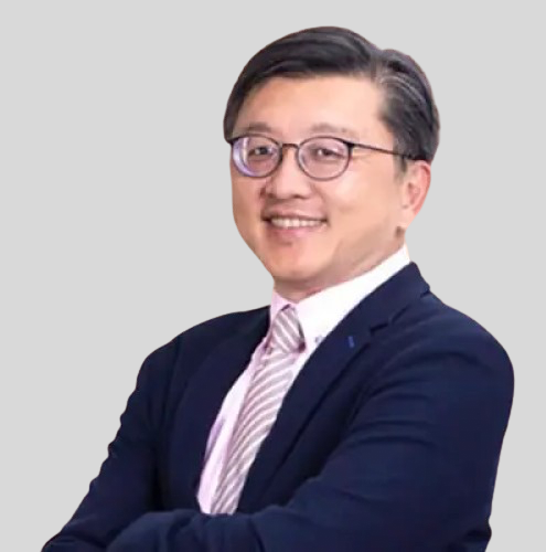
Yu-Po Wang, Ph.D.
Yu-Po Wang received Ph.D. in Mechanical Engineering from Binghamton University, State University of New York , U.S.A.
In 1997, he started career at Gintic Institute of Manufacturing Technology in Singapore.
He joins SPIL in 1998 and leads the R&D Package Application and Technology Support Team in substrate/package design, material characterization and advanced package.
Dr. Wang has strong knowledge and experience in packaging characterization including thermal/ electrical simulation, advanced material(co-development), design and advanced packaging development. He has over 83 patents in US.
IEEE Electronics Packaging Society Board of Governors (BoG) member from 2025
IEEE Electronics Packaging Society Taipei Chapter Executive Committee from 2025
09:15 – 09:45
Keynote
The New Era in Si Photonics
AI has been extending its influence in nearly every aspect of our daily endeavors; but, the power consumption seems to be the accompanied pain as the industry continue to push for ever- increasing computing power.
Over the years, among other things, Si Photonics has been heralded as a breakthrough in power saving.
However, so far, it appears to lack large volume production for >100G optical solution.
The debut of the 200G CPO with MRM is the watershed for the new era in Si photonics.
This presentation will address the driving force of the new era along with the illustration of critical aspects in Si photonics device manufacturing, followed by the introduction of technology platforms that are intended to power the AI acceleration.
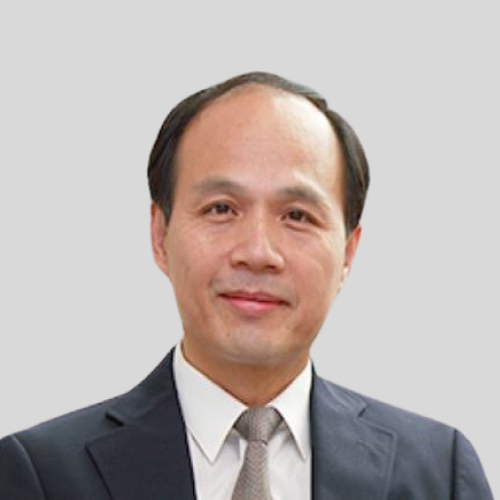
C.S. Yoo, Ph.D
TSMC
C.S. is a 30+ years’ veteran of semiconductor industry.
Ever since joined TSMC, he has been working in various technology R&D fields and Operations.
He took various managerial positions in RD Process Module, SRAM, DRAM and Embedded DRAM.
CS also led TSMC Mask RD and Operation Division before taking the position of VP in Specialty Technology RD.
CS received his PhD in Chemical Engineering from WPI (Worcester Polytechnic Institute)
Company Profile
TSMC pioneered the pure-play foundry business model when it was founded in 1987, and has been the world’s leading dedicated semiconductor foundry ever since. The Company supports a thriving ecosystem of global customers and partners with the industry’s leading process technologies and portfolio of design enablement solutions to unleash innovation for the global semiconductor industry. With global operations spanning Asia, Europe, and North America, TSMC serves as a committed corporate citizen around the world.
TSMC deployed 288 distinct process technologies, and manufactured 11,878 products for 522 customers in 2024 by providing the broadest range of advanced, specialty and advanced packaging technology services. The Company is headquartered in Hsinchu, Taiwan. For more information please visit https://www.tsmc.com.

09:45 – 10:05
Keynote
Next-Generation Silicon Photonics and 3-D Technologies for Scaling AI Systems
In this presentation, we will outline our vision for deeply integrating optical interconnects into the package, interposer, and wafer level, leveraging scaled Silicon Photonics and 3D technologies to implement high-density sub-pJ/bit optical transceivers. We will share some recent results from our ongoing research and development efforts on advanced optical devices, packaging and assembly.

Joris Van Campenhout
imec
Joris Van Campenhout is Fellow Silicon Photonics at imec and senior director of imec’s industry-affiliation R&D program on Optical I/O, which targets the development of scalable short-reach optical interconnect technology based on silicon photonics. Prior to joining imec in 2010, he was with IBM’s TJ Watson Research Center (USA), where he developed silicon electro-optic switches. He obtained a PhD degree in Electrical Engineering from Ghent University (Belgium) in 2007, for his work on heterogeneous integration of InP lasers on silicon. Joris has been granted 15+ patents and has authored or co-authored over 100 papers in the field of silicon integrated photonics, which have received 15000+ citations.
Company Profile
Imec is a world-leading research and innovation hub in advanced semiconductor technologies. Leveraging its state-of-the-art R&D infrastructure and the expertise of over 6,500 employees, imec drives innovation in semiconductor and system scaling, artificial intelligence, silicon photonics, connectivity, and sensing.
Imec’s advanced research powers breakthroughs across a wide range of industries, including computing, health, automotive, energy, infotainment, industry, agrifood, and security. Through IC-Link, imec guides companies through every step of the chip journey – from initial concept to full-scale manufacturing – delivering customized solutions tailored to meet the most advanced design and production needs.
Imec collaborates with global leaders across the semiconductor value chain, as well as with technology companies, start-ups, academia, and research institutions in Flanders and worldwide. Headquartered in Leuven, Belgium, imec has research facilities in Belgium, across Europe and the USA, and representation on three continents. In 2024, imec reported revenues of €1.034 billion.
Further information on imec can be found at www.imec-int.com.
10:05 – 10:25
From AI to Edge: Advanced Packaging Innovations and Challenges
As AI applications gradually expand from cloud-based data centers to edge computing, TSMC’s 3DFabric™ plays a pivotal role in driving continuous advancements in AI and edge technologies.
TSMC develops comprehensive technology solutions to support customer innovation, speed up product development cycles, and provide advanced 3DIC manufacturing capabilities.
As chip designs increase in density, size, and functionality, the challenges such as HBM integration, reliability, and thermal management arise. TSMC continuously improves technologies like CoWoS®, delivering greater flexibility, enhanced routability, and effective thermal solutions to address the needs of future high-power, high-integration systems.

Kathy Yan, Ph.D.
TSMC
Kathy Yan, currently Director of New Technology & System Integration, Advance Packaging and Test at TSMC. She is now in charge of new CoWoS-R organic interposer technology RD development for high speed HPC application, advanced packaging mechanical and thermal simulation & validation. She has been also managing new product co-development projects for system customers, across multiple packaging architecture including InFO POP, InFO-SOW, CoWoS-S and CoWoS-R. In addition She is the key player in TSMC 3D Fabric Alliance as the Memory Eco-system program owner. Prior to joining TSMC, she spend most of her career at Intel Advanced packaging RD and Medtronic technology Center in Arizona, US. She has a PhD in Electrical Engineering and Master in Material Science from Auburn University.
Company Profile
TSMC pioneered the pure-play foundry business model when it was founded in 1987, and has been the world’s leading dedicated semiconductor foundry ever since. The Company supports a thriving ecosystem of global customers and partners with the industry’s leading process technologies and portfolio of design enablement solutions to unleash innovation for the global semiconductor industry. With global operations spanning Asia, Europe, and North America, TSMC serves as a committed corporate citizen around the world.
TSMC deployed 288 distinct process technologies, and manufactured 11,878 products for 522 customers in 2024 by providing the broadest range of advanced, specialty and advanced packaging technology services. The Company is headquartered in Hsinchu, Taiwan. For more information please visit https://www.tsmc.com.

10:30 – 11:30
Networking and Coffee Break
Business Meeting Slot 1&2
11:35 – 11:55
Innovations Driving HBM Roadmap
The presentation delves into the advancements and innovations driving High Bandwidth Memory (HBM) roadmap.
It highlights the exponential growth of AI models and the increasing complexity requiring more memory for training.
It discusses the importance of AI in revolutionizing various aspects of human life and the role of Micron’s memory and storage solutions in accelerating AI.

Boon Ong
Micron Technology
Boon-Pin Ong (Boon) leads the Advanced Packaging Technology Development (APTD) in Micron Taiwan, focusing on enablement of advanced packaging technology roadmaps for memory and storage solutions.
Prior to his current role, Boon headed Micron’s DRAM Technology Development in Taiwan responsible for delivery of the industry’s first samples of 1γ (1-gamma), sixth-generation (10nm-class) DRAM node-based DDR5 memory.
Boon has been with the company for 20 years and served in Micron’s global semiconductor manufacturing and technology development sites in Singapore, the United States, Japan, and Taiwan.
Company Profile
Micron is a world leader in innovative memory solutions that transform how the world uses information. For over 40 years, our company has been instrumental to the world’s most significant technology advancements, delivering optimal memory and storage systems for a broad range of applications.
11:55 – 12:15
Future of AI Hardware Enabled by Advanced Packaging
Chiplet architectures are fundamental to the continued economic viable growth of power efficiency of AI hardware and edge computing. The slowing of Moore’s law has also placed advanced packaging at the critical juncture of technology-architecture intersection driving unique product capabilities. New heterogeneous architectures like 2.5D architectures and 3D Hybrid bonded architectures driving AMD’s industry leading advanced technology roadmap to enable power, performance, area, and cost (PPAC) will be discussed. Other topics including Chiplets for AI, challenges and solutions for large chiplet modules etc. will also be discussed.
Raja Swaminathan, Ph.D.
AMD
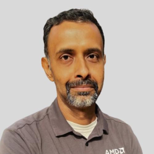
Dr. Raja Swaminathan is the Corporate Vice President of Packaging at AMD, spearheading the development of AMD’s advanced packaging and heterogeneous integration roadmap. With a distinguished career spanning roles at Intel, Apple, and now AMD, Dr. Swaminathan’s expertise in design-technology co-optimization and dedication to optimizing power, performance, area, and cost (PPAC) have led to significant technological advancements such as EMIB, Apple’s Mx packages, 3D V-Cache, and 3.5D architectures for AI accelerators. Dr. Swaminathan holds a PhD from Carnegie Mellon University and an undergraduate degree from IIT Madras. With over 100 patents and more than 40 published papers to their name, Dr. Swaminathan was recently recognized as an IEEE Fellow and serves as a technical advisor to multiple startups. His unwavering commitment to heterogeneous integration continues to drive the boundaries of silicon technology.
Company Profile
For 50 years, AMD has driven in high-performance computing, graphics, and visualization technologies – the building blocks for gaming, immersive platforms, and the datacenter. Hundreds of millions of consumers, leading Fortune 500 businesses and cutting-edge scientific research facilities around the world rely on AMD technology daily to improve how they live, work and play. AMD employees around the world are focused on building great products that push the boundaries of what is possible. For more information about how AMD is enabling today and inspiring tomorrow, visit AMD (NASDAQ:AMD) on their website, blog, Facebook and Twitter pages.

12:15 – 12:35
Technologies in Edge AI: From AI Chip Design to Chiplets Integration
Edge Artificial Intelligence (Edge AI) has emerged as a transformative paradigm, enabling real-time data processing and decision-making at the edge of networks, close to data sources. As the demand for high-bandwidth and energy-efficient edge computing grows, innovations across the hardware stack—from chip design to chiplet integration—are becoming critical. Traditional SoC designs are increasingly constrained by power, thermal, and scaling limits. In response, designers are adopting heterogeneous integration strategies, leveraging specialized processing units such as NPUs (Neural Processing Units), TPUs (Tensor Processing Units), and DSPs (Digital Signal Processors) optimized for AI workloads. Chiplets enable greater scalability, flexibility, and reuse, significantly reducing design complexity and time-to-market for edge AI solutions. Here we share chip design tailored for Edge AI, highlights the opportunities and challenges associated with chiplet-based architectures, and discusses future directions in design methodologies, and interconnect. ITRI has complete 12” process line for 3D/2.5D and fan-out process including a 2.5 µm fine-pitch Cu/oxide hybrid bonding structure, 12” wafer-to-wafer hybrid bonding at a low temperature of 200°C without thermal compression, and some use cases demonstrated for IIoT application

Wei-Chung Lo, Ph.D
Industrial Technology Research Institute (ITRI)
Dr. Lo received his Ph.D. from National Taiwan University and joined Industrial Technology Research Institute to work in advanced electronic packaging, such as WLP, 3D IC/3D stacking, fan-out, heterogeneous integration technology for more than 20 years, 85 papers and 40 patent granted. Currently, he also serves as TWG chair of IoT Chapter of IEEE Heterogenous Integration Roadmap(HIR) and chairman of International Microelectronics Assembly and Packaging Society (IMAPS)-Taiwan chapter.
Company Profile
ITRI is a world-leading applied technology research institute with more than 6,000 outstanding employees. Its mission is to drive industrial development, create economic value, and enhance social well-being through technology R&D. Founded in 1973, it pioneered in IC development and started to nurture new tech ventures and deliver its R&D results to industries. ITRI has set up and incubated companies such as TSMC, UMC, Taiwan Mask Corp., Epistar Corp., Mirle Automation.

12:40 – 14:00
Lunch Break
Day 1 Afternoon Session Moderator
Yu-Hua Chen, Ph.D.
Unimicron Technology Corp
Education:
Experience:
Company Profile
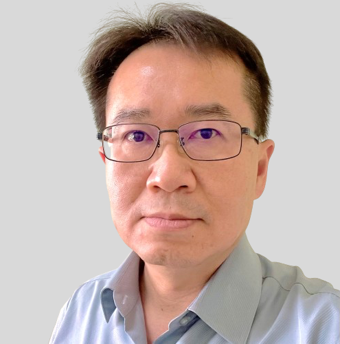
Founded in 1990, Unimicron is a world leading company of printed circuit board (PCB) and IC carrier (substrate) manufacturing. Major products include PCBs, high density interconnection (HDI) boards, flexible PCBs, rigid flex PCBs, and IC substrates. Product applications include AI, HPC data center infrastructure (server, networking), smartphones, PC/NB, optical modules, automotive and more. Unimicron’s global footprint encompass manufacturing sites and/or service centers in Taiwan, China, Germany, Japan and Thailand, delivering high value-added, high quality and high productivity innovation and services to our global customers.
Company Products & Services
Unimicron’s high-end substrate solutions, FCBGA and FCCSP, provide our valued customers the technologies crucial in meeting today’s fast-growing development of AI, HPC applications. Our customer-oriented service, high quality standards, and innovative breakthroughs have helped Unimicron achieve the honor of No.1 ranking among the global substrate suppliers by market share for the 9th consecutive year since Y2016.

14:05 – 14:50
Moderator
Hamid Azimi, Ph.D.
Marvell Technology
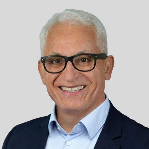
Dr. Hamid R. Azimi is Senior Vice President of Advanced Packaging and Foundry at Marvell. In this role, he leads the development and deployment of next-generation packaging technologies and foundry strategies to support Marvell’s data infrastructure products.
Prior to joining Marvell, Hamid spent nearly 30 years at Intel, where he most recently served as Corporate Vice President and Director of Substrate Packaging Technology Development. He led global R&D and manufacturing teams and delivered industry-leading innovations including die-embedded panel level fanout, EMIB and glass packaging for AI and high-performance computing.
A recognized pioneer in semiconductor packaging, Hamid holds over 40 U.S. patents, including the patent on first-generation organic flip-chip ABF-based substrate. He has received multiple Intel Achievement Awards and is widely known for building high-performing, inclusive teams and mentoring future industry leaders.
Hamid earned a Ph.D. and M.S. in Materials Science from Lehigh University and a B.S. in Materials Engineering from Sharif University of Technology.
Company Profile
We believe that infrastructure powers progress. That execution is as essential as innovation. That better collaboration builds better technology. At Marvell, We go all in with you.
Focused and determined, we unite behind your goals as our own. We leverage our unrivaled portfolio of infrastructure technology to identify the best solution for your unique needs. And we sit shoulder-to-shoulder with your teams to build it. Agile in our thinking, and our partnerships, we look for unexpected connections that deliver a competitive edge and reveal new opportunities. At Marvell, we’re driven by the belief that how we do things matters just as much as what we do. Because, with a foundation built on partnership, anything is possible.


Panelist
Raja Swaminathan, Ph.D.
AMD
Dr. Raja Swaminathan is the Corporate Vice President of Packaging at AMD, spearheading the development of AMD’s advanced packaging and heterogeneous integration roadmap. With a distinguished career spanning roles at Intel, Apple, and now AMD, Dr. Swaminathan’s expertise in design-technology co-optimization and dedication to optimizing power, performance, area, and cost (PPAC) have led to significant technological advancements such as EMIB, Apple’s Mx packages, 3D V-Cache, and 3.5D architectures for AI accelerators. Dr. Swaminathan holds a PhD from Carnegie Mellon University and an undergraduate degree from IIT Madras. With over 100 patents and more than 40 published papers to their name, Dr. Swaminathan was recently recognized as an IEEE Fellow and serves as a technical advisor to multiple startups. His unwavering commitment to heterogeneous integration continues to drive the boundaries of silicon technology.
Company Profile
For 50 years, AMD has driven in high-performance computing, graphics, and visualization technologies – the building blocks for gaming, immersive platforms, and the datacenter. Hundreds of millions of consumers, leading Fortune 500 businesses and cutting-edge scientific research facilities around the world rely on AMD technology daily to improve how they live, work and play. AMD employees around the world are focused on building great products that push the boundaries of what is possible. For more information about how AMD is enabling today and inspiring tomorrow, visit AMD (NASDAQ:AMD) on their website, blog, Facebook and Twitter pages.

Panelist
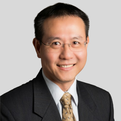
Jim Li, Ph.D.
ASE
Company Profile
ASE is the leading global provider of semiconductor manufacturing services in assembly and test. With a proven track record spanning almost 40 years, ASE today is at the forefront of flexible, powerful, integration technologies that achieve criteria for improved power, performance, area, and cost requirements. Our comprehensive toolbox leveraging innovative technologies, such as die interconnection, wafer level fan out, embedded devices, conformal and compartmental shielding, integrated antenna, and others, are being refined and enhanced to support future generations of system integration. Heterogenous Integration through SiP is enabling significant innovation across dynamic application areas including AI, 5G, automotive, mobile, IoT and more. Our industry is driven by innovation, and through ASE’s miniaturization technologies, we are enabling transformative solutions that are literally changing lives, from health to transportation, from Robotics to AI, from IoT to 5G.
Website: ase.aseglobal.com

Panelist
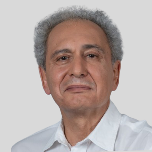
Babak Sabi, Ph.D.
AWS Annapurna Labs
Dr. Babak Sabi is VP of Technology at AWS/Annapurna Lab. Babak joined AWS in 2024 after 40 years in Intel. Babak was Senior Vice President and the General Manager of Assembly & Test Technology Development (ATTD) at Intel Corporation. Since 2009, he has been responsible for the company’s packaging, assembly, and test process technology development. During Babak’s tenure in ATTD 2.5D and 3D Advanced Packages were developed and ramp to high Volume Manufacturing. Additionally ATTD team made many advancement in Substrate and Test Technology.
Prior to leading ATTD, Babak oversaw Intel’s Corporate Quality Network from 2002 to 2009 where he led product reliability, customer satisfaction and quality business practices.
Babak joined Intel in 1984 after receiving Babak his Ph.D. in solid state electronics from Ohio State University in 1984.
Company Profile
Launched in 2006, Amazon Web Services (AWS) began exposing key infrastructure services to businesses in the form of web services — now widely known as cloud computing. The ultimate benefit of cloud computing, and AWS, is the ability to leverage a new business model and turn capital infrastructure expenses into variable costs. Businesses no longer need to plan and procure servers and other IT resources weeks or months in advance. Using AWS, businesses can take advantage of Amazon’s expertise and economies of scale to access resources when their business needs them, delivering results faster and at a lower cost.
Today, Amazon Web Services provides a highly reliable, scalable, low-cost infrastructure platform in the cloud that powers hundreds of thousands of businesses in 190 countries around the world. With data center locations in the U.S., Europe, Singapore, and Japan, customers across all industries are taking advantage of our low cost, elastic, open and flexible, secure platform.


Panelist
Onto Innovation
Mike Rosa is chief marketing officer (CMO) and senior vice president responsible for strategy at Onto Innovation. Prior to his current role, Mike served as CMO for Applied Materials ICAPS and Advanced Packaging Groups, where he was responsible for leadership of strategic and technical marketing, marketing communications, charting device segment inflection roadmaps and providing strategic business development support toward M&A activities. He has over 25 years’ experience in semiconductor engineering and technology, with roles that span device design and fabrication, equipment development, marketing and sales. His technical qualifications include B.Eng. (Hons) and Ph.D. degrees in Microelectronic Engineering and an MBA with dual majors in Marketing and Business Strategy. Mike has authored over 40 journal and conference publications and holds over 29 U.S. patents
Company Profile
Onto Innovation is a leader in process control, combining global scale with an expanded portfolio of leading-edge technologies that include: Un-patterned wafer quality; 3D metrology spanning chip features from nanometer scale transistors to large die interconnects; macro defect inspection of wafers and packages; elemental layer composition; overlay metrology; factory analytics; and lithography for advanced semiconductor packaging. Our breadth of offerings across the entire semiconductor value chain helps our customers solve their most difficult yield, device performance, quality, and reliability issues. Onto Innovation strives to optimize customers’ critical path of progress by making them smarter, faster and more efficient. Headquartered in Wilmington, Massachusetts, Onto Innovation supports customers with a worldwide sales and service organization.
General Telephone: +1 978 253 6200
General email: info@ontoinnovation.com
Website: www.ontoinnovation.com

Panelist
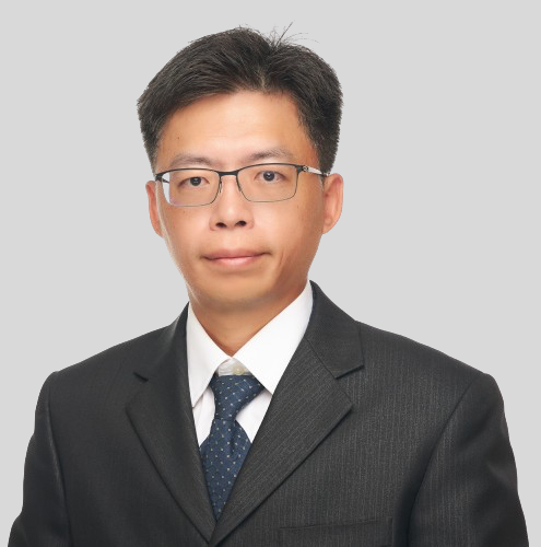
Jim Lin, Ph.D.
Powertech Technology Inc.
Dr. Jim Lin is Vice President of Advanced Technology & Wafer Level Package Operation. He is in charged of advanced packaging R&D, Business and Operation in PTI. Prior to BU head, Dr. Lin was AVP of Memory Packaging Research & Development. Dr. Lin joined PTI in 2006, led the development of memory packaging technology. Developed technologies including 8 to 32 chips memory stacking package, system integrated package of SSD, Package on Package(PoP), Heterogeneous multi-chip package(MCP), 3D TSV interconnection High Bandwidth Memory(HBM) and Fan-out Panel Level Package (FOPLP). Dr. Lin received his M.S. and Ph.D. degree both from National Tsing Hua University in Power Mechanical Engineering.
Company Profile
Powertech Technology Inc. (PTI), the world’s leading OSAT, was founded in 1997. We serve the international customers with services including chip bumping, chip probing, IC assembly, final testing, burn in, and system level assembly. In 2017 PTI expanded the production base to Japan to serve the local automotive electronics and IoT market. And in 2018, PTI began the construction of the newest Fan Out Panel Level Package manufacturing facility in Hsinchu Science Park.
PTI has over 18,000 employees world wide, and manufacturing facility located in Taiwan, China and Japan. PTI dedicates her efforts in developing advanced technologies, while carrying on as the world’s leading memory packaging and testing solution provider. Through strategic alliances and resource integration, PTI group relentlessly marches onward in the semiconductor packaging and testing field.
We drive our future growth with outstanding quality, cost, and delivery. Promise, Technology, and Integration represents our core values. With our ideaology, strategy, and core values, PTI stands as the world class OSAT.
Company Products & Services
PTI offers the services inculding Final test, Chip Probe, IC Packaging, Module Assembly, Quality Management. And provide wide range of technology solution for IC packaing including Panel Level Fan Out, TSV solution, Bumping, Flip chip, Antenna in Package.
-Panel Level Fan Out
Fan-out packaging is going to become the mainstream for high-end device application, especially for multi-die, heterogeneous integration for both active & passive devices. High density interconnect, excellent performance in electrical performance and power consumption can also be achieved by panel FO. PTI’ Panel level FO packaging offers the merits of high production efficiency with better utilization & unit output in comparison to wafer level FO.
Solution: CHIEFS® / CLIP® / PiFO® / BF2O®
TSV Solution-3DIC
3D IC is one kind of heterogeneous technology which is integrated vertically by Si wafers or chips. The interconnection is composed by u-bumps and Through Silicon Via (TSV). TSV fabrication is regarded as the heart of 3D IC because it provides the advantages of shortening the interconnection path, high function density, low power consumption, smaller form factor and high performance; these benefits make 3D IC get commercial success in some specific applications, such like HPC and AI.
TSV Solution-CMOS Image Sensor
CMOS Image Sensor (CIS) is an electronic device that converts an optical image into an analog signal. Recently, the most attractive is stack-CIS, that BSI CIS, memory wafer and Image Signal Processor(ISP) wafer are vertically integrated and higher performance, lower power consumption would be the advantages for high-end application.
Bumping
Wafer bumping is a metal bump that grows on a wafer, and each bump is an IC signal contact. Unlike conventional interconnection through wire-bond, bond pads are placed at peripheral area , IO pads for bumping could be distributed all over the surface of the chip, thus chip size could be shrunk and electrical path could be optimized.
14:50 – 15:10
Keynote
Wafer Test Challenges in the HPC AI Era
The generative AI is driving significant growth in the semiconductor industry. To deliver the massive computing power required to train AI models, new chip designs pack increasingly more transistors and adopt disaggregated chiplet architectures, connected by advanced packaging technologies. This presentation will describe the some of the test challenges and opportunities for HPC AI products.
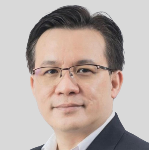
Kam Lee
TSMC
Kam currently serves as Senior Director at TSMC Advanced Packaging Technology and Service, which he joined in 2022. He specifically manages the TSMC Testing RD, Testing operations and backend turnkey operations. He has extensive experience in semiconductor industry, having worked 27 years at Intel, in various roles in technology development, product development and high volume manufacturing. He previously held the role of Vice President of Intel product development and engineering.
Company Profile
TSMC pioneered the pure-play foundry business model when it was founded in 1987, and has been the world’s leading dedicated semiconductor foundry ever since. The Company supports a thriving ecosystem of global customers and partners with the industry’s leading process technologies and portfolio of design enablement solutions to unleash innovation for the global semiconductor industry. With global operations spanning Asia, Europe, and North America, TSMC serves as a committed corporate citizen around the world.
TSMC deployed 288 distinct process technologies, and manufactured 11,878 products for 522 customers in 2024 by providing the broadest range of advanced, specialty and advanced packaging technology services. The Company is headquartered in Hsinchu, Taiwan. For more information please visit https://www.tsmc.com.

15:10 – 15:20
Advanced Probing Materials for Semiconductor Testing
Testing of high-performance computer chips demands specialized probe needle material solutions, capable of handling high current densities, thermal management challenges as well as mechanical property requirements. To tackle these challenges Heraeus Precious Metals developed a new alloy class – Palysium C+ – utilizing optimized order disorder transitions in Pd-Cu based alloys to form so called superlattice structures. Palysium C+ features exceptional conductivity, while maintaining very good mechanical properties which, in turn, results in a significant increase in the CCC-value compared to state-of-the-art Pd-Cu based solutions, making Palysium C+ the ideal material solution for advanced testing applications.

Matthias Wegner, Ph.D.
Heraeus Precious Metals
Formal education:
Physics studies @ University of Muenster, Germany – Institute of Materials Physics
PhD in Materials Physics @ University of Muenster, Germany – Institute of Materials Physics
Professional career:
2015 – 2016 Post Doc @ University of Muenster – Institute of Materials Physics
2017 – 2021 Materials Scientist Innovation @ Heraeus Precious Metals – Functional Materials
2021 – 2022 Team Lead Innovation @ Heraeus Precious Metals – Functional Materials
2022 – 2024 Head of Innovation @ Heraeus Precious Metals – Functional Materials
2024 – today Global Head of Innovation @ Heraeus Precious Metals – Functional Materials
2018 – today IP-Manager @ Heraeus Precious Metals – Functional Materials
Company Profile
Heraeus Precious Metals is globally leading in the precious metals industry. The company is part of the Heraeus Group and covers the value chain from trading to precious metals products to refining and recycling. It has extensive expertise in all platinum group metals as well as gold and silver. With more than 3,000 employees at 17 sites worldwide, Heraeus Precious Metals offers a broad portfolio of products that are essential for many industries such as the automotive, chemicals, semiconductor, pharmaceutical, hydrogen and jewelry industry.
Company Products & Services
Heraeus offers top-quality solutions and products based on many years of experience and technical expertise. They are a reliable development partner for customers and find the best solutions for their requirements. One area for precious metals in semiconductors is the use of special alloys for semiconductor wafer testing, also known as probing. Heraeus offers a wide range of probe pin materials, from precipitation-hardened PdAgCu alloys to high-strength PtNi alloys. Probe pin materials made by Heraeus can be applied to any probe card type.

15:20 – 15:30
Revolutionary Acoustic Microscopic Imaging (AMI) Technology for Wafer-Level and Advanced Packaging
Pre-Recorded

Bryan Schackmuth
Nordson TEST & INSPECTION
Senior Product Line Manager for Acoustic Technologies at Nordson Test & Inspection for the Optical Sensor & Metrology division (OSM). Overseeing the development and implementation of advanced acoustic inspection systems tailored for the semiconductor market.
Introduction of SpinSAM™ Acoustic Micro Imaging system for wafer applications. This innovative solution utilizes a unique spin scan method enabling very high throughput for acoustic inspection. Its modular design allows for simultaneous scanning of up to four wafers for continuous operation while ensuring minimal downtime during maintenance.
Integration of Artificial Intelligence (AI) and Machine Learning (ML) in the acoustic inspection processes. Leveraging AI/ML to revolutionize image analysis within acoustic inspection aiming to significantly reduce the time required for complex sample analysis.
Company Profile
Nordson Test & Inspection offers its SMT & Semiconductor customers a robust product portfolio, including Acoustic, Optical and both Manual and Automated X-ray Inspection systems, X-ray Component Counting systems and Semiconductor measurement sensors. Nordson Test & Inspection is uniquely positioned to serve its customers with best-in-class precision technologies, passionate sales and support teams, global reach, and unmatched consultative applications expertise.
About Nordson
Nordson Corporation (Nasdaq: NDSN) is an innovative precision technology company that leverages a scalable growth framework through an entrepreneurial, division-led organization to deliver top tier growth with leading margins and returns. The Company’s direct sales model and applications expertise serves global customers through a wide variety of critical applications. Its diverse end market exposure includes consumer non-durable, medical, electronics and industrial end markets. Founded in 1954 and headquartered in Westlake, Ohio, the Company has operations and support offices in over 35 countries. Visit Nordson on the web at https://www.nordson.com/, https://x.com/nordson_corp or https://www.facebook.com/nordson/.
Company Products & Services
High Accuracy. High Resolution. High Speed.
Nordson Test & Inspection manufactures world-class metrology and inspection systems & sensors. Our inspection metrology equipment meets the highest standards for electronic assembly and semiconductor applications. Acoustic, Optical, Bond Test, X-ray Components, Manual X-ray, and Automated X-ray systems enable you to identify even the smallest defects at high resolution and capture critical measurements. Wireless Semiconductor Sensors can significantly improve semiconductor tool setup and maintenance.
We design, develop, and manufacture innovative inspection & metrology equipment for a wide range of industries, including AI, Server & 5G, Consumer, Automotive, Power & Energy, Sensors & LED, Aerospace & Defense and Medical.
Our key segments include Advanced SMT, Advanced Packaging, Front-End semiconductor, Mid-End semiconductor, and Back-End semiconductor.
The right inspection & metrology equipment can elevate your product quality. If you’re looking to save time and money, and improve your yields, processes, and productivity, of the semiconductors or the electronics you manufacture, our inspection equipment can help you ensure exceptional quality every time.

15:35 – 16:35
Networking and Coffee Break
Business Meeting Slot 3&4
16:40 – 16:50
The Challenges of Heterogeneous Integration
The Challenges in Heterogeneous Integration: Warpage, Singulation Defects, ESD/EOS/EMI, and Wet Process Issues
Heterogeneous integration (HI) combines multiple chip technologies within a single package, pushing the limits of materials, manufacturing, and reliability. Among the key challenges are warpage, singulation defects (such as Si chipping and cracking), electrostatic discharge (ESD), electrical overstress (EOS), electromagnetic interference (EMI), and issues related to wet process etching and cleaning.

Eric Lee
Scientech
Eric Lee is the CEO of Scientech Corp. and Chairman of Yayatech. He joined Scientech in 2004, following nearly a decade at UMC, where he held positions in both Taiwan and Singapore from 1995 to 2004.
In addition to his leadership roles at Scientech and Yayatech, Eric serves as President of the International Semiconductor Executive Summit (ISES) Taiwan. He is also a part-time professor in the Advanced Packaging Master’s Program at National Taiwan University of Science and Technology.
Eric contributes actively to the industry through his roles as a member of the SEMI Taiwan Advanced Packaging Committee and as a director of the Taiwan Electronic Equipment Industry Association.
Company Profile
Scientech Corporation was established in Taipei, Taiwan in 1979.
What we do: Industries we serve: Semiconductor (front-end, back-end and GaAs), Flat Panel Display, LED, Data Storage, Scientific Instruments and high-tech related industries.
Being a leading semiconductor equipment and wafer reclaim supplier in Taiwan, Scientech Corporation has launched the development of wet process equipment in 2003. Scientech has successively supported customers in LED, Mini/Micro LED, compound semi and power components such as IGBT, SiC and GaN industries, as well as advanced packaging process such as Bumping, Fan-out, Chip-On-Wafer and so on. Our wet process equipment has been successfully verified in the latest Chiplet’s 2.5D/3D packaging process technology and smoothly introduced into mass production.

16:50 – 17:00
Accelerating the AI Era
The AI era has arrived and to accelerate it, the AP industry and supply chain needs to innovate at a torrid pace to stay in tandem with the exponential growth of the Gen AI and AI ASIC computing trajectory. As a first mover in AP, ASMPT has been investing in the last 10 years to lead in end-to-end solutions for chiplets heterogeneous integration of the most advanced chip architecture in CoWoS and HBM. The AP industry is undergoing a “Power of N” transformation where fine interconnect pitch shall shrink rapidly along with thinner and bigger packaging formats, demanding breakthrough technologies in materials, process and equipment. This signals a need for a robust supply chain and ecosystem to continuously re-invent advanced packaging technologies to enable AI scaling.
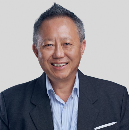
Choon Khoon Lim
ASMPT Semiconductor Solutions
LIM Choon Khoon (CK) is a Senior Vice President and Chief Executive Officer of Semiconductor Solutions Advanced Packaging (AP).
CK’s career spans key engineering, manufacturing, and regional functional and global general management roles with several global semiconductor companies. As Chief Executive Officer of the Segment’s AP Business Group, he helps provide the industry’s leading first-level interconnect technologies covering leading AP First Level Interconnect (FLI) technologies for logic, HBM, Si Photonics & Co-Packaged Optics, wafer die singulation solution for advanced fabricated wafers and Panel ECD for fine Line/Space organic and glass substrate & Wafer PVD, that are well-positioned to serve and to scale with the most demanding AP needs.
CK holds a Bachelor of Science (Honours) in Production Engineering and Production Management degree from the University of Nottingham, United Kingdom
Company Profile
ASMPT Limited, founded in 1975, is headquartered in Singapore and is listed in Hong Kong Stock Exchange since 1989.
ASMPT is the only company in the world that offers high-quality equipment for all major steps in the electronics manufacturing process – from carrier for chip interconnection to chip assembly and packaging to SMT. No other supplier offers a comparable range and depth of process expertise.
Semiconductor Solutions Segment Business of ASMPT offers a diverse product range from bonding to molding and trim & form to the integration of these activities into complete in-line systems for the microelectronics, semiconductor, camera modules, advanced packaging, photonics, and optoelectronics industries.
The group has successfully established itself as the leading player in the back-end assembly and packaging market with its innovative solutions and constant focus on customer value creation.


Joshua Yoo
Core Insight, Inc.
Yong Hoon (Joshua) Yoo has been involved in the static control industry since 1994 for ionization, ESD measurement and high voltage power business operation in semiconductor, flat panel displays and automotive industry. He has been a member of EOS/ESD Association since 2000 and served as an Elected Board of Director in 2016 – 2018. He is the founder and president of Korea EOS/ESD Association since 2011. He is a member of Institute of Electronics and Information Engineers (Korean IEEE) since 2021. He is serving industry as Korea President of International Semiconductor Executive Summits (ISES) since 2024.
He started his volunteering activities on EOS/ESD Association since 2013 as an active working group members and technical program committee members of annual symposium for multiple events of ESD Association. With his leadership, Korea EOS/ESD Association very strongly presents and annual events over 10 years. He is pioneer for flat panel display (FPD) static issue analysis and resolved problems. In recently, he found a root cause of ESD yield losses in AI chip manufacturing environment and improved yield over double digits.
He is an iNARTE certified ESD Engineer in 2007 and the EOS/ESD Association certified Professional ESD Program Manager in 2011. He has 14 patents for ionization system and ESD testing technologies.
Company Profile
Core Insight is a leading company for EOS/ESD control with technical expertise and key insights for Advanced Package Device application. Heterogeneous Integration technology revolutionary achieved new device era. This new technology also brought new challenges that much less ESD sensitivity before it finished package device. Core Insight has prepared to meet new level of ESD control with world best ionization solution which no one else have. Core Insight has understanding device technology, manufacturing process and ESD control know-how for Advanced Package Device handling.

17:10 – 17:20
PulseForge Photonic Debonding: Validated Advantages for Semiconductor Manufacturing

Vikram Turkani
PulseForge
Vikram Turkani, serves as the Director of Technology Partnerships and Strategic Business Development at PulseForge Inc., a prominent technology company specializing in advanced packaging solutions based in Austin, Texas. In this pivotal role, Vikram is instrumental in steering the development and implementation of cutting-edge technologies at PulseForge. Through close collaboration with global technology partners, he ensures the successful transition of these state-of-the-art solutions into practical applications within the market.
Beyond driving the development of innovative technologies, Vikram actively engages with PulseForge’s customers, facilitating the seamless adoption of these innovations on a large scale. In addition to his professional pursuits, Vikram enjoys hiking Texas hill country and exploring the vibrant Austin food scene.
Company Profile
PulseForge, Inc. develops and manufactures state-of-the-art flashlamp-based tools that deliver energy in a precise and targeted manner to enable innovation in industrial manufacturing. Our expertise and tools empower our customers to explore novel materials and manufacturing methodologies, driving dynamic and efficient production at an industrial scale.

17:20 – 17:25
Closing Address
I.S.I.G.
International Semiconductor Industry Group (ISIG)
Established in 2010, the International SemiconductorIndustry (I.S.I.G.) is a prestigious & trusted associationwithin the semiconductor industry, renowned fororchestrating major regional summits across the globe,ranging from the U.S, the Middle East & Asia via ourdivision, the International Semiconductor ExecutiveSummits (I.S.E.S.). Our summits are fully endorsed bylocal governments and leading companies in all areas ofthe semiconductor supply chain.
Moreover, I.S.E.S. serves as the Premier platform for senior executives in technology, manufacturing, and R&D from diverse semiconductor companies, technology providers, and affiliated industries.
Our events are instrumental helping to shed light onto key industry trends, drive innovation and influence key decisions to help shape, and advance the growth of the semiconductor sector.
17:30 – 18:45
Cocktail Reception sponsored by
GTI (Green Technology Investments)
Green Technology Investments LLC (GTi), headquartered in Scottsdale, Arizona, is a pioneering force in the semiconductor industry. With a focus on innovative remanufacturing and software solutions, GTi aims to revolutionize how businesses access advanced technology. Since its inception, in 2012, GTi has been committed to providing high-quality equipment and expert services to its global clientele. With offices strategically located in North America, Europe, and Asia, GTi is well-positioned to meet the needs of customers worldwide. By investing in research and development, GTi continues to expand the capabilities of remanufactured equipment and software, making cutting-edge technology more accessible and affordable for businesses of all sizes. GTi’s impact on the semiconductor industry is profound, enabling businesses to compete effectively in today’s dynamic market landscape.
Green Technology Investments LLC (GTi) offers a comprehensive range of products and services tailored to the semiconductor industry’s evolving needs. Specializing in remanufacturing and software solutions, GTi provides access to advanced technology at a more affordable price point. Their product lineup includes remanufactured semiconductor equipment such as CD-SEM, DR-SEM metrology systems, and MASK systems, ensuring high-quality performance and significant cost savings compared to new systems. In addition to equipment, GTi offers ready-to-ship spare parts, expert service support, and foundry capabilities to enhance customer experience and satisfaction. With a relentless focus on innovation and customer satisfaction, GTi is dedicated to empowering businesses of all sizes with the tools they need to thrive in today’s competitive global market.
18:45 – 19:00
Dinner Check-in
19:00 – 21:00
Gala Dinner and Award Ceremony
Gala Dinner Sponsored by:
Welcome Dinner Speaker

Simon Liu, Ph.D.
Camtek
Experience
Education
National Tsing Hua University
Ph.D., Physics, Nuclear Science 1988 – 1991
As taking on the role of General Manager of Camtek Ltd.’s Taiwan branch since 2013, leading to gain a clear understanding of the company’s existing business model and the challenges it faced, laying the foundation for a comprehensive growth strategy.
The growth strategy began delivering measurable results in 2015, when the company achieved its highest global annual sales in its sector. Since then, it has maintained an impressive 30% year-over-year growth and received numerous industry accolades.
This management philosophy has led to remarkable outcomes. The Taiwan branch has consistently achieved strong annual performance, rapidly expanded its market share, and emerged as a market leader in Taiwan’s advanced semiconductor back-end packaging, testing, inspection, and metrology sector.
Company Profile
Camtek is a developer and manufacturer of high-end inspection and metrology equipment for the semiconductor industry.
With manufacturing facilities in Israel and Germany, and eight offices around the world, Camtek provides state of the art inspection and metrology solutions in line with customers’ requirements.
Company Products & Services
Camtek has three product lines: Eagle and Hawk for inspection and 3D metrology and MicroProf for metrology.
Camtek’s inspection solutions provide comprehensive coverage for semiconductor manufacturing, supporting front-side inspection at sub-micron defect levels, as well as backside and edge inspection. Camtek’s 3D metrology solutions deliver precise measurements for micro-bump coplanarity and height, handling up to 500 million bumps per wafer. Our advanced metrology capabilities also cover critical parameters such as RDL CD/Overlay, TSV, topography, TTV, warp/bow, and layer thickness, ensuring comprehensive process control and high-quality manufacturing.

End of content
End of content