9-11 December 2025
Muscat, Oman
No posts
13-14 May 2025 - Taipei


08:00 – 08:40
Registration
Day 2 Morning Session Moderator

Kuan-Neng Chen, Ph.D.
NYCU
Dr. Kuan-Neng Chen is Dean of International College of Semiconductor Technology and Chair Professor at Institute of Electronics at National Yang Ming Chiao Tung University (NYCU) in Taiwan. He received his Ph.D. degree in Electrical Engineering and Computer Science, as well as his M.S. degree in Materials Science and Engineering, both from Massachusetts Institute of Technology (MIT). Dr. Chen has held several prominent positions including Vice President for International Affairs, Associate Dean of International College of Semiconductor Technology at NYCU, Program Director of the Micro-Electronics Program at National Science and Technology Council in Taiwan, Adjunct R&D Director at Industrial Technology and Research Institute (ITRI), and Research Staff Member at IBM Thomas J. Watson Research Center.
Dr. Chen has received numerous awards and honors throughout his career, including IEEE EPS Exceptional Technical Achievement Award, IMAPS William D. Ashmon – John A. Wagnon Technical Achievement Award, National Industrial Innovation Award, MOST/NSTC Outstanding Research Award (twice), MOST/NSTC Futuristic Breakthrough Technology Award (twice), Pan Wen Yuan Foundation Outstanding Research Award, CIE Outstanding Professor Award, CIEE Outstanding Professor Award, and IBM Invention Achievement Awards (5 times). He has authored over 400 publications, including 3 books and 7 book chapters, and holds 88 patents. Dr. Chen served as Guest Editor for the MRS Bulletin, IEEE Transactions on Components, Packaging, and Manufacturing Technology, and Materials Science in Semiconductor Processing, and has held leadership roles in various conferences and committees, such as IEEE IITC General Chair. Dr. Chen is Fellow of National Academy of Inventors (NAI), IEEE, IET, IMAPS, and CIEE and member of Phi Tau Phi Scholastic Honor Society.
Additionally, Dr. Chen is Specially Appointed Professor at Institute of Tokyo Science (previously Tokyo Tech). His current research interests focus on three-dimensional integrated circuits (3D IC), advanced packaging, and heterogeneous integration.
Company Profile
NYCU was founded on the idea that, in a great university, people work across the disciplines to solve real-world problems. At our university, putting this idea into practice requires integrating Chiao Tung’s strengths in information and communications technology with Yang Ming’s strengths in biomedical research. It also requires contributing to fields located at the intersection of these research areas, for example, digital medicine and bioinformatics. And it requires training our students in such a way that the next generation will not be as constrained by disciplinary boundaries as the previous one.
At NYCU, we are striving to be a great university that transcends disciplinary divides to solve the increasingly complex problems that the world faces. We will continue to be guided by the idea that we can achieve something much greater together than we can individually. After all, that was the idea that led to the creation of our university in the first place.

08:40 – 09:10
AI Powered Innovation: Driving the Next Wave of Semiconductor Breakthrough
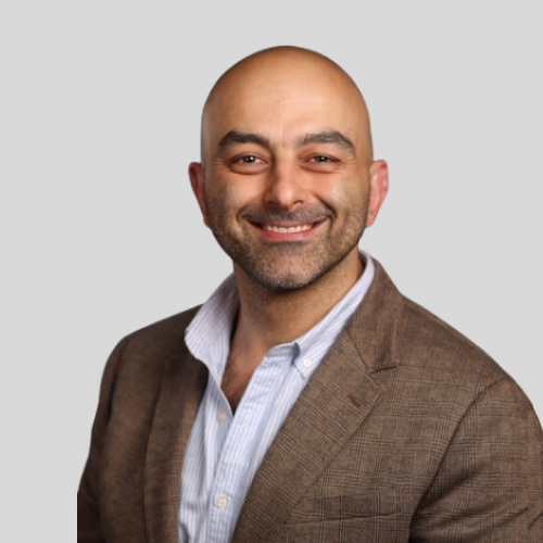
M. Ashkan Seyedi, Ph.D.
NVIDIA
Ashkan Seyedi received a dual bachelor’s in electrical and computer engineering from the University of Missouri-Columbia and a Ph.D. from University of Southern California working on photonic crystal devices, high-speed nanowire photodetectors, efficient white LEDs, and solar cells. With a decade of industry experience at Intel, Hewlett Packard Enterprise and now NVidia, Dr. Seyedi has been working on developing high-bandwidth, efficient optical interconnects for exascale, and high-performance computing applications.
Company Profile
Since its founding in 1993, NVIDIA (NASDAQ: NVDA) has been a pioneer in accelerated computing. The company’s invention of the GPU in 1999 sparked the growth of the PC gaming market, redefined computer graphics, ignited the era of modern AI and is fueling the creation of the metaverse. NVIDIA is now a full-stack computing company with data-center-scale offerings that are reshaping industry.
09:10 – 09:40
Future Packaging/System Challenges for AI Data Centers
Artificial Intelligence is the largest technology transformation since Internet revolutionized communication and business. This transformation has required advancement in Si, Memory, Packaging, and System technologies. In this talk, the packaging and system technology challenges will be presented.
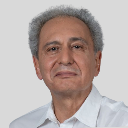
Babak Sabi, Ph.D.
AWS Annapurna Labs
Dr. Babak Sabi is VP of Technology at AWS/Annapurna Lab. Babak joined AWS in 2024 after 40 years in Intel. Babak was Senior Vice President and the General Manager of Assembly & Test Technology Development (ATTD) at Intel Corporation. Since 2009, he has been responsible for the company’s packaging, assembly, and test process technology development. During Babak’s tenure in ATTD 2.5D and 3D Advanced Packages were developed and ramp to high Volume Manufacturing. Additionally ATTD team made many advancement in Substrate and Test Technology.
Prior to leading ATTD, Babak oversaw Intel’s Corporate Quality Network from 2002 to 2009 where he led product reliability, customer satisfaction and quality business practices.
Babak joined Intel in 1984 after receiving Babak his Ph.D. in solid state electronics from Ohio State University in 1984.
Company Profile
Launched in 2006, Amazon Web Services (AWS) began exposing key infrastructure services to businesses in the form of web services — now widely known as cloud computing. The ultimate benefit of cloud computing, and AWS, is the ability to leverage a new business model and turn capital infrastructure expenses into variable costs. Businesses no longer need to plan and procure servers and other IT resources weeks or months in advance. Using AWS, businesses can take advantage of Amazon’s expertise and economies of scale to access resources when their business needs them, delivering results faster and at a lower cost.
Today, Amazon Web Services provides a highly reliable, scalable, low-cost infrastructure platform in the cloud that powers hundreds of thousands of businesses in 190 countries around the world. With data center locations in the U.S., Europe, Singapore, and Japan, customers across all industries are taking advantage of our low cost, elastic, open and flexible, secure platform.

09:40 – 10:40
Networking and Coffee Break
Business Meeting Slot 5&6
Advanced Packaging Legends Forum:
The Evolution of Advanced Packaging: Milestones, Challenges, and Future Opportunities (from 2015 and beyond 2025)
10:45 – 11:35

Moderator
Salah Nasri
International Semiconductor Industry Group (ISIG)
Salah Nasri is the CEO and Co-Founder of the International Semiconductor Industry Group (ISIG), a global organization founded in 2010 that connects and empowers semiconductor decision-makers through strategic leadership platforms, executive summits, and collaborative initiatives. ISIG has become a trusted global hub for industry leaders driving innovation and progress across the semiconductor value chain.
With extensive experience across the semiconductor sector, Salah has played a pivotal role in fostering global collaboration among industry leaders. Under his leadership, ISIG has evolved into one of the most influential communities in the semiconductor ecosystem—bringing together executives, innovators, and policymakers across regions including the United States, Europe, Asia, and the Middle East.
Salah has been instrumental in expanding ISIG’s reach and impact, curating high-level summits and initiatives that drive dialogue and progress across critical areas such as semiconductor manufacturing, AI, MEMS, automotive electronics, and advanced packaging. His vision continues to position ISIG as a key platform for thought leadership, networking, and strategic industry alignment.
Earlier in his career, Salah held positions at Credit Suisse, Goldman Sachs, Worldwide Business Research, and the International Business Development Group. He studied International Relations and Economics at Oxford University and Loughborough University, and in 2024 became a Stanford University alumnus after completing the Stanford Executive Program. In addition to his role at ISIG, Salah also serves on the Advisory Board of Atlant3D, a pioneer in atomic-layer advanced manufacturing solutions.
Company Profile
Established in 2010, the International SemiconductorIndustry (I.S.I.G.) is a prestigious & trusted associationwithin the semiconductor industry, renowned fororchestrating major regional summits across the globe,ranging from the U.S, the Middle East & Asia via ourdivision, the International Semiconductor ExecutiveSummits (I.S.E.S.). Our summits are fully endorsed bylocal governments and leading companies in all areas ofthe semiconductor supply chain.
Moreover, I.S.E.S. serves as the Premier platform for senior executives in technology, manufacturing, and R&D from diverse semiconductor companies, technology providers, and affiliated industries.
Our events are instrumental helping to shed light onto key industry trends, drive innovation and influence key decisions to help shape, and advance the growth of the semiconductor sector.

Panelist
Babak Sabi, Ph.D.
AWS Annapurna Labs
Dr. Babak Sabi is VP of Technology at AWS/Annapurna Lab. Babak joined AWS in 2024 after 40 years in Intel. Babak was Senior Vice President and the General Manager of Assembly & Test Technology Development (ATTD) at Intel Corporation. Since 2009, he has been responsible for the company’s packaging, assembly, and test process technology development. During Babak’s tenure in ATTD 2.5D and 3D Advanced Packages were developed and ramp to high Volume Manufacturing. Additionally ATTD team made many advancement in Substrate and Test Technology.
Prior to leading ATTD, Babak oversaw Intel’s Corporate Quality Network from 2002 to 2009 where he led product reliability, customer satisfaction and quality business practices.
Babak joined Intel in 1984 after receiving Babak his Ph.D. in solid state electronics from Ohio State University in 1984.
Company Profile
Launched in 2006, Amazon Web Services (AWS) began exposing key infrastructure services to businesses in the form of web services — now widely known as cloud computing. The ultimate benefit of cloud computing, and AWS, is the ability to leverage a new business model and turn capital infrastructure expenses into variable costs. Businesses no longer need to plan and procure servers and other IT resources weeks or months in advance. Using AWS, businesses can take advantage of Amazon’s expertise and economies of scale to access resources when their business needs them, delivering results faster and at a lower cost.
Today, Amazon Web Services provides a highly reliable, scalable, low-cost infrastructure platform in the cloud that powers hundreds of thousands of businesses in 190 countries around the world. With data center locations in the U.S., Europe, Singapore, and Japan, customers across all industries are taking advantage of our low cost, elastic, open and flexible, secure platform.

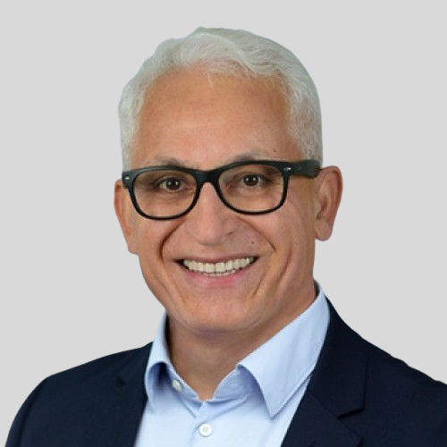
Panelist
Hamid Azimi, Ph.D.
Marvell Technology
Dr. Hamid R. Azimi is Senior Vice President of Advanced Packaging and Foundry at Marvell. In this role, he leads the development and deployment of next-generation packaging technologies and foundry strategies to support Marvell’s data infrastructure products.
Prior to joining Marvell, Hamid spent nearly 30 years at Intel, where he most recently served as Corporate Vice President and Director of Substrate Packaging Technology Development. He led global R&D and manufacturing teams and delivered industry-leading innovations including die-embedded panel level fanout, EMIB and glass packaging for AI and high-performance computing.
A recognized pioneer in semiconductor packaging, Hamid holds over 40 U.S. patents, including the patent on first-generation organic flip-chip ABF-based substrate. He has received multiple Intel Achievement Awards and is widely known for building high-performing, inclusive teams and mentoring future industry leaders.
Hamid earned a Ph.D. and M.S. in Materials Science from Lehigh University and a B.S. in Materials Engineering from Sharif University of Technology.
Company Profile
We believe that infrastructure powers progress. That execution is as essential as innovation. That better collaboration builds better technology. At Marvell, We go all in with you.
Focused and determined, we unite behind your goals as our own. We leverage our unrivaled portfolio of infrastructure technology to identify the best solution for your unique needs. And we sit shoulder-to-shoulder with your teams to build it. Agile in our thinking, and our partnerships, we look for unexpected connections that deliver a competitive edge and reveal new opportunities. At Marvell, we’re driven by the belief that how we do things matters just as much as what we do. Because, with a foundation built on partnership, anything is possible.

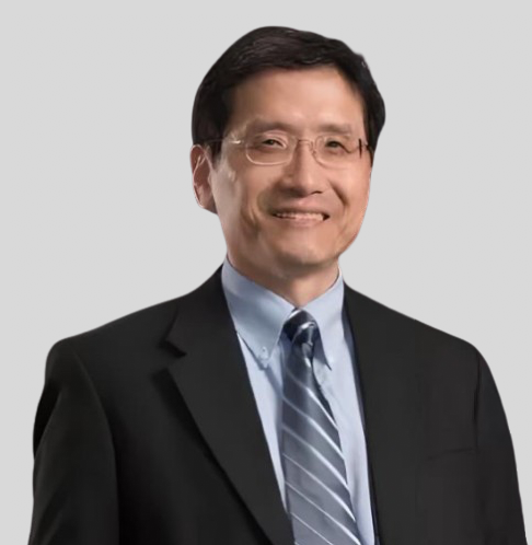
Panelist
Jerry Tzou
TSMC
Jerry Tzou recently retired from TSMC, where he wrapped up as Director of Advanced Packaging Business Development. He spearheaded the strategic growth of TSMC’s 3DFabric® platform— CoWoS®, InFO, TSMC-SoIC®, TSMC-SoW™, and COUPE™ for Co-Packaged Optics (CPO) —tying it to TSMC’s advanced silicon innovations. This work fueled next-generation applications in AI-driven high-performance computing, mobile, automotive, and IoT. Through synergistic collaboration with customers and partners inside and out, he drove significant revenue growth in advanced packaging.
Jerry’s 40-year semiconductor career included diverse roles at TSMC, a stint as VP of Product Operations at Global Unichip Corporation (GUC), a TSMC-affiliated design foundry, and advanced packaging work at Apple, National Semiconductor, Cirrus Logic, and select Silicon Valley startups. With a Master’s in Materials Science and Engineering from UC Berkeley, his expertise spans semiconductor packaging, operations, and business development.
Company Profile
TSMC pioneered the pure-play foundry business model when it was founded in 1987, and has been the world’s leading dedicated semiconductor foundry ever since. The Company supports a thriving ecosystem of global customers and partners with the industry’s leading process technologies and portfolio of design enablement solutions to unleash innovation for the global semiconductor industry. With global operations spanning Asia, Europe, and North America, TSMC serves as a committed corporate citizen around the world.
TSMC deployed 288 distinct process technologies, and manufactured 11,878 products for 522 customers in 2024 by providing the broadest range of advanced, specialty and advanced packaging technology services. The Company is headquartered in Hsinchu, Taiwan. For more information please visit https://www.tsmc.com.


Panelist
International Semiconductor Industry Group (ISIG)
Education :
Experience :
Company Profile
Established in 2010, the International SemiconductorIndustry (I.S.I.G.) is a prestigious & trusted associationwithin the semiconductor industry, renowned fororchestrating major regional summits across the globe,ranging from the U.S, the Middle East & Asia via ourdivision, the International Semiconductor ExecutiveSummits (I.S.E.S.). Our summits are fully endorsed bylocal governments and leading companies in all areas ofthe semiconductor supply chain.
Moreover, I.S.E.S. serves as the Premier platform for senior executives in technology, manufacturing, and R&D from diverse semiconductor companies, technology providers, and affiliated industries.
Our events are instrumental helping to shed light onto key industry trends, drive innovation and influence key decisions to help shape, and advance the growth of the semiconductor sector.


Panelist
Mostafa Aghazadeh
Chiplink Consulting LLC
Mostafa Aghazadeh is a seasoned industry leader and the President of Chiplink Consulting LLC, where he advises companies on advanced packaging technology and manufacturing.Previously, he spent 40 years at Intel, holding various leadership roles in Assembly & Test Technology Development. As a Corporate Vice President, he led Intel’s assembly process, materials, and equipment technology development.He currently serves on the technical advisory boards of BESI, Brewer Science, and IMEC and previously chaired the INEMI Board of Directors. He was also a member of Arizona State University’s New Economy Initiative and the School of Manufacturing Systems and Networks Industry Advisory Board.
Company Profile
Provide consulting services in the areas of microelectronics advanced packaging technology, manufacturing, and supply chain including process, equipment, and materials.
Company Products & Services
Consulting Services

11:40 – 12:00
The Optical Connectivity Paradigm Shift: Where We Are and Where We’re Going
Large scale AI computing is creating immense strain on compute infrastructure. At the core of AI computation are bottlenecks in data movement and connectivity. Electrical interconnects are reaching their limits of performance and power efficiency, and optical connectivity is poised to solve these challenges. In this talk, we will review the opportunities and challenges as the industry works to deliver a new generation of optical connectivity in computing fabrics.

Mark Wade, Ph.D.
Ayar Labs
Mark is Chief Executive Officer and Co-Founder of Ayar Labs. His prior roles at Ayar Labs include Chief Technology Officer and Senior Vice President of Engineering. He is recognized as a pioneer in photonics technologies and, prior to founding the company, led the team that designed the optics in the world’s first processor to communicate using light. He and his co-founders invented breakthrough technology at MIT and UC Berkeley from 2010-2015 which led to the formation of Ayar Labs. He holds a PhD from University of Colorado.
Company Profile
Ayar Labs is disrupting the traditional performance, cost, and efficiency curves of the semiconductor and computing industries by driving a 1000x improvement in interconnect bandwidth density at 10x lower power. Ayar Labs’ patented approach uses industry standard cost-effective silicon processing techniques to develop high speed, high density, low power optical based interconnect “chiplets” and lasers to replace traditional electrical based I/O. The company was founded in 2015 and is funded by a number of domestic and international venture capital firms as well as strategic investors. For more information, visit www.ayarlabs.com.
Address: 695 River Oaks Parkway, San Jose, CA 95134
Phone: 650-963-7200
Email: info@ayarlabs.com

12:00 – 12:20
The Development of Silicon Photonics in Optical Communications, and its Challenges
AI GPU link is playing an increasingly critical role in data centers and high-performance edge computing systems. Among the enabling technologies, silicon photonics is rapidly advancing—particularly in pluggable optical transceivers and the emerging field of co-packaged optics. Currently, external laser sources (ELS) are the mainstream approach for optical input. Assembling laser chip and fiber onto PICs remains a bottleneck. In the talk, I’ll also discuss Internal Laser Source (ILS) on PIC and 2D fiber array with metalens.
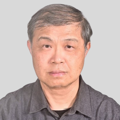
David Chang, Ph.D.
AuthenX. Inc
Dr. David Chang is the CTO of AuthenX Inc., where he leads the research and development division, focusing on silicon photonics, optoelectronics, and optical communication technologies.
Prior to his industry career, Dr. Chang was a professor at National Central University, Taiwan, where his research centered on nano-optics and optoelectronics. His work has contributed to advancements in optical communications, solid-state lighting, and biophotonics. He has authored over 100 research papers and holds more than 30 patents.
Dr. Chang earned his Ph.D. in Materials Engineering from Massachusetts Institute of Technology.
Company Profile
Founded in 2019, AuthenX is an optoelectronic product development company specializing in Silicon Photonics and III-V Photonics key components. Our core technologies include optical design, high-speed circuits, precision packaging, and system integration. Leveraging industrial chain integration, we provide solutions and products for next-generation data centers, AI GPU systems, FTTX, and PON applications.
Company Products & Services
Our products and services include 400Gbps, 800Gbps, and up to 1.6Tbps optical transceivers, as well as high-power ELS modules for CPO in data centers and AI GPU systems. In silicon photonics, we focus on the hybrid integration of Optical I/O on PICs, including laser-to-PIC and PIC-to-FAU integration, aiming to improve PIC I/O packaging tolerance and throughput. Our products are applicable in fields ranging from PON and FTTX to data centers and AI GPU systems.

12:20 – 12:30
Introduction of Lightmatter
Discover how a leading silicon photonics company is shaping the future of high-speed interconnect. This brief talk will highlight Lightmatter’s mission, market focus, and the strategic role its products play in enabling next-generation technologies.
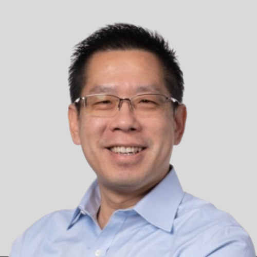
Eric Yeh
Lightmatter
With over 20 years of experience in product marketing and management, Eric is a leader in driving innovation and product adoption across the semiconductor industry. His technical expertise spans photonics, processors, interconnects, and networking. All of these technologies are instrumental in shaping his vision for today’s advanced computing systems.
Throughout his career, Eric has held key management and leadership roles at Broadcom, MediaTek, and Marvell, consistently working at the forefront of technological innovation. At Marvell, he led the product team at the Networking Business Unit, where he played a pivotal role in expanding the company’s presence in the Ethernet Switching market.
Today, Eric serves as Head of Product Marketing at Lightmatter, where he is spearheading efforts to bring silicon photonics to XPUs and AI networking, with a focus on accelerating AI performance while maximizing power efficiency.
Company Profile
Lightmatter is leading the revolution in AI data center infrastructure and enabling the next giant leaps in human progress. The company was founded in 2017 out of MIT, with two of its co-founders – CEO Nick Harris, Ph.D. and Chief Scientist Darius Bunandar, Ph.D. – renowned as preeminent scientists in the field. Lightmatter has raised $850 million in funding by leading investors including Fidelity, Google Ventures, Sequoia, Spark, T Rowe Price, and Viking, and was most recently valued at $4.4 billion. Initially founded in Boston, Lightmatter moved its headquarters to Mountain View in 2023. It currently employs 230 employees across its headquarters in Silicon Valley, as well as offices in Boston, Toronto, Oregon and Arizona.
Company Products & Services
The company’s groundbreaking Passage™ platform—the world’s first 3D-stacked silicon photonics engine—connects thousands to millions of processors at the speed of light. Designed to eliminate critical data bottlenecks, Lightmatter’s technology enables unparalleled efficiency and scalability for the most advanced AI and high-performance computing workloads, pushing the boundaries of AI infrastructure.

12:35 – 13:40
Lunch Break
13:45 – 13:55
Disruption in Semiconductor Industry
For over 40 years, AlixPartners has been helping clients confront disruption. Increasingly, cycles of disruption have displaced economic cycles as the primary business challenge.
Disruption is the new economic driver. We will share the results our 6th annual AlixPartners Disruption Index, with particular insights on how CEOs and senior executives of the semiconductor industry perceive major disruptions, opportunities and challenges in this exciting field around the globe.
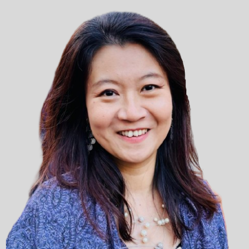
Janet Tang
AlixPartners
Janet brings 20 years of a variety of industry experience such as as chief strategy officer (CSO) of a Global 500 company, oversight of P&L responsibilities, service in consulting leadership, role as a software architect, and engagements in entrepreneurship. Janet is known for successfully driving complex transformations in technology firms and telcos, turning around cost centers into profit centers, building transformative go-to-market engines, and coaching next generations of client leaders. Her early career as a software architect in Silicon Valley also gave her hands-on experience in R&D and product management.
Janet has a Master of Science in Computer Science from Stanford University. She has served as a board member of the University of Toronto Engineering Alumni Network and as chair of the network’s Nomination and Governance Committee.
Company Profile
AlixPartners is a results-driven global consulting firm that specializes in helping businesses respond quickly and decisively to their most critical challenges—from urgent performance improvement to complex restructuring, from risk mitigation to accelerated transformation. These are the moments when everything is on the line—a sudden shift in the market, an unexpected performance decline, a time-sensitive deal, a fork-in-the-road decision. We stand shoulder to shoulder with our clients until the job is done, and only measure our success in terms of the results we deliver.
Company Products & Services
Clients call us when they need pragmatism and cut-through to solve their most complex challenges arising from a continually disrupted world. Our services cover Artificial Intelligence, Corporate Strategy & Transformation, Data Governance, ESG, Growth, Investigations, Disputes & Advisory Services, Mergers & Acquisitions, Organizational Transformation, Supply-Chain Management & Operations, Technology, Transformative Leadership and Turnaround and Restructuring.


Romain Fraux
Yole Group
Romain Fraux serves as the Chief Research Officer at Yole Group, leveraging his extensive expertise in the semiconductor industry to lead the development of the organization’s global operations.
He oversees a team of analysts dedicated to exploring the semiconductor landscape, encompassing “More Moore” and “More than Moore” technologies, semiconductor manufacturing, and the global supply chain, with the goal of identifying innovations and business opportunities.
Under Romain’s leadership, Yole Group’s international team delivers comprehensive services, including market research, technology and strategy analysis, reverse engineering and cost assessment, and module performance evaluation. These insights empower Yole Group’s clients to make informed decisions about their future business and manufacturing strategies in the semiconductor, photonics, and electronics sectors.
In his cross-functional executive role, Romain represents Yole Group during key client engagements and regularly shares the organization’s strategic vision at leading international conferences. With over 15 years at Yole Group, he has been instrumental in shaping its position as a thought leader in the industry.
Romain holds a bachelor’s degree in Electrical Engineering from Heriot-Watt University in Edinburgh (Scotland), a master’s degree in Microelectronics from the University of Nantes (France), and an MBA (IEMN – IAE, France).
Company Profile
Yole Group is a leading international market research and strategy consulting firm, delivering in-depth analyses across market trends, technology developments, teardowns, and reverse costing. Leveraging deep semiconductor expertise, its team of analysts also provides custom consulting services, offering strategic, technical, and market insights tailored to address specific business challenges and opportunities.

14:15 – 14:20
I.S.I.G. Closing Remarks
14:25 – 16:25
Networking Reception
14:25 – 14:55
Business Meeting Slot 7
End of content
End of content