9-11 December 2025
Muscat, Oman
No posts
21-22 April - Silicon Valley


07:15 – 08:15
Registration
08:15 – 08:30
I.S.I.G. 15th Year Anniversary Opening
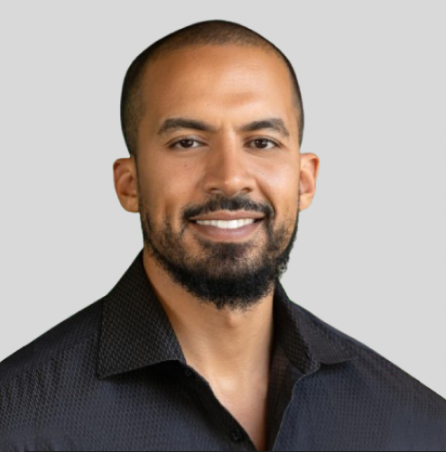
Salah Nasri
International Semiconductor Industry Group (ISIG)
Salah Nasri is the CEO and Co-Founder of the International Semiconductor Industry Group (ISIG), a global organization founded in 2010 that connects and empowers semiconductor decision-makers through strategic leadership platforms, executive summits, and collaborative initiatives. ISIG has become a trusted global hub for industry leaders driving innovation and progress across the semiconductor value chain.
With extensive experience across the semiconductor sector, Salah has played a pivotal role in fostering global collaboration among industry leaders. Under his leadership, ISIG has evolved into one of the most influential communities in the semiconductor ecosystem—bringing together executives, innovators, and policymakers across regions including the United States, Europe, Asia, and the Middle East.
Salah has been instrumental in expanding ISIG’s reach and impact, curating high-level summits and initiatives that drive dialogue and progress across critical areas such as semiconductor manufacturing, AI, MEMS, automotive electronics, and advanced packaging. His vision continues to position ISIG as a key platform for thought leadership, networking, and strategic industry alignment.
Earlier in his career, Salah held positions at Credit Suisse, Goldman Sachs, Worldwide Business Research, and the International Business Development Group. He studied International Relations and Economics at Oxford University and Loughborough University, and in 2024 became a Stanford University alumnus after completing the Stanford Executive Program. In addition to his role at ISIG, Salah also serves on the Advisory Board of Atlant3D, a pioneer in atomic-layer advanced manufacturing solutions.
Company Profile
Established in 2010, the International SemiconductorIndustry (I.S.I.G.) is a prestigious & trusted associationwithin the semiconductor industry, renowned fororchestrating major regional summits across the globe,ranging from the U.S, the Middle East & Asia via ourdivision, the International Semiconductor ExecutiveSummits (I.S.E.S.). Our summits are fully endorsed bylocal governments and leading companies in all areas ofthe semiconductor supply chain.
Moreover, I.S.E.S. serves as the Premier platform for senior executives in technology, manufacturing, and R&D from diverse semiconductor companies, technology providers, and affiliated industries.
Our events are instrumental helping to shed light onto key industry trends, drive innovation and influence key decisions to help shape, and advance the growth of the semiconductor sector.
08:35 – 08:50
Welcome

Saeed Amidi
Plug and Play Tech Center
Saeed is a seasoned investor and executive with over 30 years of experience growing businesses in numerous industries, including real estate, bottled water, packaging, and technology investing. Following the early success of his various businesses, The Amidi Group initially purchased a building in Palo Alto and decided to rent the extra office spaces to startups.
As the CEO and founder of Plug and Play, Saeed applies his passion for the tech industry daily by working with forward-thinking partners and the best global startups to facilitate positive change worldwide. Since Plug and Play’s launch in 2006, the company has worked with over 90,000 startups, made over 2,000 investments, and boasts over 30 unicorns including Dropbox, PayPal, Lending Club, N26, and Honey. Similar to his unexpected success with the “Lucky Building,” Saeed considered himself lucky overall when he moved to Silicon Valley in the late 70s, where he was then unaware of the ecosystem it would become.
Company Profile
Plug and Play is the ultimate innovation platform. Our mission is to build the world’s leading innovation platform and make innovation open to anyone, anywhere. We do this by connecting entrepreneurs, corporations, and investors worldwide.
Over the past 15 years, we have brought together 35,000+ startups, 500+ world-leading corporations, and hundreds of venture capital firms, universities, and government agencies across 20+ industries.
We are active in 50+ locations globally, including the U.S., China, France, Germany, South Africa, Singapore, Indonesia, Brazil, and more.
Together with our partners, we are creating a unique ecosystem designed to facilitate meaningful introductions, invest in startups, and bring together key stakeholders.
The industries we focus on include Agtech, Animal Health, Brand & Retail, Crypto & Digital Assets, Energy, Enterprise, Fintech, Food & Beverage, Health, Insurtech, IoT, Maritime, Media & Ad, Mobility, New Materials & Packaging, Real Estate & Construction, Smart Cities, Supply Chain, Sustainability, and Travel & Hospitality.

08:55 – 09:05
Follow the Data: Timely and Targeted
In this presentation, Mr. Sherman is excited to introduce the ISIG Chips & Wafers Data Reports for the first time to our members.
The ISIG data reports are designed as a reliable and actionable resource for semiconductor companies; providing timely and targeted data to help our members make more informed decisions.

Simi Sherman
International Semiconductor Industry Group (ISIG)
Simi Sherman is Co-Founder and CEO of Chips & Wafers, a semiconductor data and research platform, and VP of Research with ISIG.
After six years at a Buy-Side global equities Hedge Fund, where he was a Partner and led semiconductor research, Simi Co-founded Chips & Wafers. Working together with ISIG, Chips & Wafers provides semiconductor companies and investors with timely and actionable data they utilize in making more informed decisions.
Company Profile
Established in 2010, the International SemiconductorIndustry (I.S.I.G.) is a prestigious & trusted associationwithin the semiconductor industry, renowned fororchestrating major regional summits across the globe,ranging from the U.S, the Middle East & Asia via ourdivision, the International Semiconductor ExecutiveSummits (I.S.E.S.). Our summits are fully endorsed bylocal governments and leading companies in all areas ofthe semiconductor supply chain.
Moreover, I.S.E.S. serves as the Premier platform for senior executives in technology, manufacturing, and R&D from diverse semiconductor companies, technology providers, and affiliated industries.
Our events are instrumental helping to shed light onto key industry trends, drive innovation and influence key decisions to help shape, and advance the growth of the semiconductor sector.

09:10 – 09:30
Keynote
AI Inspired. Systems Accelerated.
The shifting landscape of technology requires a multi-faceted foundry approach to keep pace with increasing workload of data centers and high-performance computing (HPC) systems. The use of chiplets and “system of chips” offer a way to unlock exponential improvements in semiconductor products. Intel Foundry is addressing these needs with decades of experience in world class manufacturing, innovative advancements in packaging and system technology optimization, delivered through a more resilient and more sustainable global supply chain. Join us as we outline how Intel Foundry is tackling the next wave of semiconductor breakthroughs.

Kevin O’Buckley
Intel Foundry
Kevin O’Buckley is senior vice president and general manager of Foundry Services at Intel Corporation. In this role, he is responsible for driving continued growth for Intel Foundry and its differentiated systems foundry offerings, which go beyond traditional wafer fabrication to include packaging, chiplet standards and software, as well as U.S.- and Europe-based capacity.
Prior to joining Intel, O’Buckley was senior vice president of Marvell’s Compute and Custom Solutions Engineering teams, developing advanced technology chips for infrastructure applications including artificial intelligence and machine learning, 5G wireless, and data center compute and networking. While at Marvell he also served as senior vice president and general manager of the company’s ASIC business, and he was a member of the board of directors at Marvell Government Solutions, developing semiconductor solutions for aerospace and defense customers.
O’Buckley joined Marvell as part of its 2019 acquisition of Avera Semiconductor, where he served as chief executive. He has also held various executive engineering and business leadership roles at Global Foundries and at IBM, where he served for more than 17 years leading technology development and manufacturing organizations.
Company Profile
Intel’s systems foundry approach offers full-stack optimization from the factory network to software. Intel and its ecosystem empower customers to innovate across the entire system through continuous technology improvements, reference designs and new standards. Intel Foundry is an independent foundry business that meets our customers’ unique product needs, including our industry-leading sort and test capabilities. Whether front-end or back-end design is needed, when integrated with our foundry co-optimized development kits based on industry-standard tools and flows and powerful silicon IPs, the result is true innovation.

09:35 – 10:35
Networking Break and Business Meetings
Coffee & Tea Break Sponsored by:
Airspace
Whether your production line is facing a shutdown, or your high-value equipment is waiting for a new component, you can’t afford a shipping delay. From life-saving organs to essential machinery components, Airspace is trusted by the world’s largest companies and most critical organizations to move their top time-sensitive shipments on time, every time.
Airspace’s proprietary AI-powered platform is the most advanced of its kind- awarded and protected by multiple patents, it provides speed, reliability, routing, tracking visibility and transparency unrivaled in time-critical logistics. It powers a 24/7/365 pro-active expert support team that understands the needs of vertical specific shipments such as those in the semiconductor business.
With offices in the United States in Southern California, Dallas, and in Europe in Amsterdam and new offices in Frankfurt, Stockholm, and Paris, London, Porto, Airspace is rapidly scaling into new markets and industries while continuing to innovate and maximize value for its customers. Backed by leading investors including Telstra, HarbourVest, Prologis, Qualcomm, Defy, and others, Airspace has raised $70M to date.
Whether your production line is facing a shutdown, or your high-value equipment is waiting for a new component, you can’t afford a shipping delay.
Airspace’s proprietary AI-powered platform is the most advanced of its kind- awarded and protected by multiple patents, it provides speed, reliability, routing and transparency unrivaled in time-critical logistics. It powers a 24/7/365 pro-active expert team that understands the specific needs of shipments such as those in the semiconductor business.
From NFO, to OBC, dedicated drives, charters and more, the Airspace technology will calculate the best routing for you, taking your specific requirements into consideration as well as automating the process to save your team valuable time.
Your supply chain is complicated — we make it easy for you.
10:40 – 11:00
High Bandwidth Memory (HBM) and Advanced Packaging in AI
As the requirement of processing data in Artificial Intelligence (AI) grows exponentially, a large capacity and high bandwidth in memory technology plays a pivotal role in the integrated AI system performances. High bandwidth memories (HBMs) has been great solutions since 2017 when HBM2 was implemented in nVIDIA P100/V100. Currently, 6th generation HBM, HBM4 is in development.The continued scaling of HBM to increase memory capacity and bandwidth and additionally to enhance thermal performance has been great challenges and required the evolutions of 3D stacking technologies. In this presentation, HBM stacking technology innovations and roadmap will be presented. HBM stacking challenges associated with next generation advanced packaging technologies will be discussed.
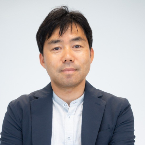
Jaesik Lee Ph.D.
SK Hynix
Dr. Jaesik Lee is Vice President of Package Engineering at SK hynix America. In this role, Jaesik is responsible for the research and development of advanced packaging for next generation High Bandwidth Memory (HBM) and pathfinding initiatives which enrich SK hynix’s innovations. He also focuses on the collaborations with customers to overcome HBM challenges associated with System in Packages (SIPs).
Prior to joining SK hynix America, Jaesik has held various key technical positions through Meta, Google, Nvidia, and Qualcomm where he drove advanced packaging technology developments, Packaging and System Co-optimization, and Manufacturing in Mobile, AI, and HPC applications. He received a PhD in mechanical engineering from University of Waterloo.
Company Profile
An AI First Mover Leading the Global AI Memory Era
With our global technology leadership, SK hynix aims to provide greater value to all stakeholders, including our customers, partner companies, investors, local communities, and employees.
Moreover, we are working to strengthen our ESG management to create even more value, by moving away from the conventional business model of seeking only economic benefits, in pursuit of more social value and a healthier governance structure.
SK hynix will grow into a Full Stack AI Memory Provider, offering customized solutions tailored to the diverse needs of global customers, covering both DRAM and NAND flash, in the era of full-scale AI.

11:05 – 11:25
Innovations driving HBM roadmap
HBM is fueling extraordinary demands of compute in AI era. In this talk, we will explore innovations that will be critical to driving HBM roadmap.

Akshay Singh Ph.D.
Micron Technology
Dr. Akshay Singh is vice president of Advanced Packaging Technology Development at Micron Technology. He leads a global team that is responsible for delivering advanced memory packaging solutions for HBM, high performance compute and AI/ML applications. Dr. Singh joined Micron in 2006 as an interposer materials engineer and since then has held number of positions of increasing responsibility in packaging design, integration and technology development. Prior to joining Micron, Dr. Singh held product development positions at Artificial Muscle, Inc. and USDA.
Dr. Singh has authored several keynote publications and patents and has served as an invited panel speaker at several conferences. Dr. Singh holds master’s and doctorate degrees in mechanical engineering from Louisiana State University, bachelor’s degree in mechanical engineering from Maharaja Sayajirao University and is a graduate of the Stanford Graduate School of Business Executive Program.
Education:
Company Profile
Micron is a world leader in innovative memory solutions that transform how the world uses information. For over 40 years, our company has been instrumental to the world’s most significant technology advancements, delivering optimal memory and storage systems for a broad range of applications.
11:30 – 11:50
Is Heterogeneous Integration (HI) ready for Artificial Intelligence (AI)?
Moore’s law has helped us for 5+ decades through monolithic integration with doubling of transistors every two years. With the introduction of deep learning in 2012, compute demand has been out pacing Moore’s law. Progress in AI over the last decade has been hardware driven with large scale models exploiting the large transistor connectivity available. More recently there appears to be a shift towards developing software efficiencies, along with hardware advances. Nevertheless, the need for more and more transistors will never cease, and hence continuation of Moore’s law becomes a necessity. Heterogenous Integration (HI) is taking the front seat to continue Moore’s law.
But is HI ready to take on this challenge for the next decade? Are we geared towards saving our planet from an energy crisis? What are some of the key technologies that we need to focus on for HI? This presentation will address some of these questions by focusing on challenges as well as recent progress.
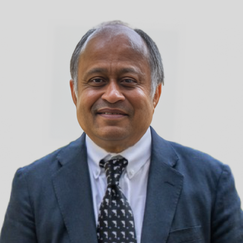
Madhavan Swaminathan, Ph.D.
Penn State University
Madhavan Swaminathan is the Department Head of Electrical Engineering and is the William E. Leonhard Endowed Chair at Penn State University. He also serves as the Director for the Center for Heterogeneous Integration of Micro Electronic Systems (CHIMES), an SRC JUMP 2.0 Center chimes.psu.edu. Prior to joining Penn State, he was the John Pippin Chair in Microsystems Packaging & Electromagnetics in the School of Electrical and Computer Engineering (ECE), Professor in ECE with a joint appointment in the School of Materials Science and Engineering (MSE), and Director of the 3D Systems Packaging Research Center (PRC) – a graduated NSF-Engineering Research Center (ERC), Georgia Tech (GT). Prior to GT, he was with IBM working on packaging for supercomputers. Prof. Swaminathan’s interdisciplinary research on semiconductor packaging and systems integration over the years have resulted in 650+ technical publications, 200+ invited presentations (seminars, keynotes, panels), 3 books, 5 book chapters, 31 patents, 33 best paper and student paper awards, 5 GT awards, 2 start-ups, and several international recognitions with the recent one being the 2024 IEEE Rao R. Tummala Electronics Packaging Award (technical field award) for “contributions to semiconductor packaging and system integration technologies that improve the performance, efficiency, and capabilities of electronic systems”. He is also the founder of the IEEE Conference on Electrical Design of Advanced Packaging and Systems (EDAPS), a premier conference sponsored by the IEEE Electronics Packaging Society (EPS). He is a Fellow of IEEE, Fellow of the National Academy of Inventors (NAI), Fellow of Asia-Pacific Artificial Intelligence Association (AAIA), and has served as the Distinguished Lecturer for the IEEE Electromagnetic Compatibility (EMC) society. He received his MS and PhD degrees in Electrical Engineering from Syracuse University, USA.
Company Profile
There’s a reason Penn State consistently ranks among the top one percent of the world’s universities. Across 24 campuses, our nearly 88,000 students and 17,000 faculty and staff know the real measure of success goes beyond the classroom—it’s the positive impact made on communities across the world. From access to state-of-the-art resources to interdisciplinary pursuits in collaborative atmospheres, a Penn State degree is more than an education. The experiences and knowledge gained here will form the foundation for the lives our students build. Their contributions to the world begin with a Penn State degree. We Are Penn State.


Roger St. Amand
Amkor Technology, Inc.
Roger has more than 30 years of experience in the semiconductor industry and became part of Amkor in 2003. During his tenure at Amkor, he has taken on various leadership positions, and he currently oversees the Chiplet /FCBGA/fcCSP business unit, along with its associated packaging technologies. Prior to joining Amkor, Roger worked at Digital Equipment Corporation and Microchip Technology. He earned a Bachelor of Science in Electrical Engineering from the University of Massachusetts and a Master of Science in Materials Science from Stanford University. Additionally, Roger is an inventor on more than 70 patents related to semiconductor processing, packaging, and applications.
Company Profile
Amkor Technology, Inc. is the world’s largest US headquartered OSAT (outsourced semiconductor assembly and test). Since its founding in 1968, Amkor has pioneered the outsourcing of IC packaging and test services and is a strategic manufacturing partner for the world’s leading semiconductor companies, foundries, and electronics OEMs. Amkor provides turnkey services for the communication, automotive and industrial, computing, and consumer industries, including but not limited to smartphones, electric vehicles, data centers, artificial intelligence and wearables. Amkor’s operational base includes production facilities, product development centers and sales and support offices located in key electronics manufacturing regions in Asia, Europe and the United States. Learn more at https://amkor.com
12:20 – 13:35
Buffet Lunch
13:40 – 14:20
Panel Session: Evolving Trends for Advanced Packaging and the Challenges for Supply Chain and End User Applications

Moderator
Monita Pau, Ph.D.
Onto Innovation
Monita Pau is currently Strategic Marketing Director for Advanced Packaging at Onto Innovation. She works with business leaders and executives to drive strategic planning and leads the development of collaborative initiatives to drive growth and innovation. With over 15 years of experience, her expertise spans across frontend and backend of line process control solutions as well as specialty materials for advanced packaging and assembly. Prior to joining Onto, she held various positions in applications engineering, marketing and strategic business development at DuPont and KLA. Monita holds a Ph.D. degree in Chemistry from Stanford University.
Company Profile
Onto Innovation is a leader in process control, combining global scale with an expanded portfolio of leading-edge technologies that include: Un-patterned wafer quality; 3D metrology spanning chip features from nanometer scale transistors to large die interconnects; macro defect inspection of wafers and packages; elemental layer composition; overlay metrology; factory analytics; and lithography for advanced semiconductor packaging. Our breadth of offerings across the entire semiconductor value chain helps our customers solve their most difficult yield, device performance, quality, and reliability issues. Onto Innovation strives to optimize customers’ critical path of progress by making them smarter, faster and more efficient. Headquartered in Wilmington, Massachusetts, Onto Innovation supports customers with a worldwide sales and service organization.
General Telephone: +1 978 253 6200
General email: info@ontoinnovation.com
Website: www.ontoinnovation.com

Panelist
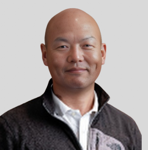
Vincent Kim, Ph.D.
Samsung
Dr. Vincent (WooPoung) Kim is the Corporate EVP, Head of Packaging at Samsung Device Solutions Research America based in San Jose, California. Dr. Kim is responsible for leading the packaging division at Samsung Device Solutions Research America, dedicated to meeting industry’s needs for advanced chip packaging in high-performance systems. Prior to joining Samsung, he served as a System Architect for Signal Integrity and Power Integrity at Apple, where he played a crucial role in developing consumer computers. Before his tenure at Apple, Dr. Kim worked as an SI Manager in Snapdragon packaging at Qualcomm. Prior to that, he was a Co-Design Engineer in the Wireless Business Unit of Texas Instruments, where he specialized in optimizing the electrical design of OMAP packages and systems. Dr. Kim also gained valuable experience as an SI Engineer at Rambus, where he designed and analyzed memory systems.
Dr. Kim received his Ph.D degree in Electrical and Computer Engineering (ECE) at Georgia Tech in 2004, and his M.S. & B.A. degrees from KAIST, Korea in 1999 and 1997.
Company Profile
Samsung Electronics Co., Ltd. engages in the manufacturing and selling of electronics and computer peripherals. The company operates through following business divisions: Consumer Electronics, Information Technology & Mobile Communications and Device Solutions. The Consumer Electronics business division provides cable television, monitor, printer, air-conditioners, refrigerators, washing machines and medical devices. The Information Technology & Mobile Communications business division offers handheld products, communication systems, computers and digital cameras. The Device Solutions business division comprises of memory, system large scale integrated circuit and foundry. The company was founded on January 13, 1969 and is headquartered in Suwon, South Korea.


Panelist
Jaesik Lee Ph.D.
SK Hynix
Dr. Jaesik Lee is Vice President of Package Engineering at SK hynix America. In this role, Jaesik is responsible for the research and development of advanced packaging for next generation High Bandwidth Memory (HBM) and pathfinding initiatives which enrich SK hynix’s innovations. He also focuses on the collaborations with customers to overcome HBM challenges associated with System in Packages (SIPs).
Prior to joining SK hynix America, Jaesik has held various key technical positions through Meta, Google, Nvidia, and Qualcomm where he drove advanced packaging technology developments, Packaging and System Co-optimization, and Manufacturing in Mobile, AI, and HPC applications. He received a PhD in mechanical engineering from University of Waterloo.
Company Profile
An AI First Mover Leading the Global AI Memory Era
With our global technology leadership, SK hynix aims to provide greater value to all stakeholders, including our customers, partner companies, investors, local communities, and employees.
Moreover, we are working to strengthen our ESG management to create even more value, by moving away from the conventional business model of seeking only economic benefits, in pursuit of more social value and a healthier governance structure.
SK hynix will grow into a Full Stack AI Memory Provider, offering customized solutions tailored to the diverse needs of global customers, covering both DRAM and NAND flash, in the era of full-scale AI.

Panelist
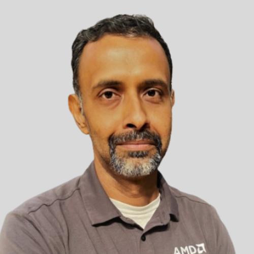
Raja Swaminathan, Ph.D.
AMD
Dr. Raja Swaminathan is the Corporate Vice President of Packaging at AMD, spearheading the development of AMD’s advanced packaging and heterogeneous integration roadmap. With a distinguished career spanning roles at Intel, Apple, and now AMD, Dr. Swaminathan’s expertise in design-technology co-optimization and dedication to optimizing power, performance, area, and cost (PPAC) have led to significant technological advancements such as EMIB, Apple’s Mx packages, 3D V-Cache, and 3.5D architectures for AI accelerators. Dr. Swaminathan holds a PhD from Carnegie Mellon University and an undergraduate degree from IIT Madras. With over 100 patents and more than 40 published papers to their name, Dr. Swaminathan was recently recognized as an IEEE Fellow and serves as a technical advisor to multiple startups. His unwavering commitment to heterogeneous integration continues to drive the boundaries of silicon technology.
Company Profile
For 50 years, AMD has driven in high-performance computing, graphics, and visualization technologies – the building blocks for gaming, immersive platforms, and the datacenter. Hundreds of millions of consumers, leading Fortune 500 businesses and cutting-edge scientific research facilities around the world rely on AMD technology daily to improve how they live, work and play. AMD employees around the world are focused on building great products that push the boundaries of what is possible. For more information about how AMD is enabling today and inspiring tomorrow, visit AMD (NASDAQ:AMD) on their website, blog, Facebook and Twitter pages.


Panelist
SkyWater Technology
Bassel Haddad is Sr Vice President and General Manager of Advanced Packaging at SkyWater Technology. He leads all aspects of SkyWater’s advanced packaging business including technology development, engineering, marketing and Florida fab operations. He is responsible for building and scaling the business serving both the defense and commercial market sectors. He is focused on strengthening collaborations with the advanced packaging ecosystem, such as equipment and material vendors, government partners and research institutes & consortia, while driving the growth trajectory of the business.
Before joining SkyWater, Haddad was with Intel since 2011 holding various engineering and business leadership roles. Most recently, he was the Vice President and General Manager of edge device and AI products, in the network and edge group. In this role, he managed a multi-billion dollar P&L, and leading innovations in edge AI and Internet of Things, or IoT. Earlier in his career, he held roles in platform architecture, silicon development, systems and software engineering, delivering leadership products to various end markets.
Haddad holds a Bachelor’s and Master’s degree in electrical engineering from Technion – Israel Institute of Technology. He is the inventor of five USPTO-issued patents in the areas of digital communication and systems architecture.
Company Profile
SkyWater (NASDAQ: SKYT) is a U.S.-based semiconductor manufacturer and a DMEA-accredited Category 1A Trusted Supplier. SkyWater’s Technology as a Service model streamlines the path to production for customers with development services, volume production and heterogeneous integration solutions in its U.S. facilities. This pioneering model enables innovators to co-create the next wave of technology within diverse categories including mixed-signal CMOS, ROICs, rad-hard ICs, MEMS, superconducting ICs, photonics and advanced packaging. SkyWater serves the growing markets of aerospace & defense, automotive, biomedical, industrial and quantum computing. For more information, visit: www.skywatertechnology.com.
14:25 – 14:45
Advanced low cost chiplet package for HPC, AI
High density interconnects is the key for achieving high bandwidth package which is required mainly for HPC and other high-end applications. Heterogeneous integration is one of the robust and cost effective solution to support the increasing demands in compute performance and memory areas. Chip level heterogeneous integration or Chiplet technology is an encouraging low cost solution for advanced Si node expensive die. These die can be from a range of wafer sizes fabricated in different technology nodes from various semiconductor sources. Chiplets are small IC dies with specialized functionality, designed to combine to make up a bigger and complex chips required for high performance applications. This advanced packaging type creates many challenges in assembly and manufacturing yield.
There are various ways of making Chiplet package depending on the end application requirement, cost and ease of supply chain. Fine line and space standard substrate, Si interposer, RDL interposer, embedded bridge die in RDL interposer, etc. are some of the popular options currently available in the market for Chiplet packaging. This paper will explore the various processes and technologies to achieve a cost effective and high performance Chiplet package.

Nokibul Islam, Ph.D.
STATS ChipPAC
Dr. Nokibul Islam is the Sr. Director of STATS ChipPAC Business Unit, where he leads product business development and advanced technology promotion. With over 21 years of experience in semiconductor product management, business development, and advanced packaging, he previously played a key role in Amkor Technology’s R&D team, focusing on product development, simulation, characterization, and process improvement. He is actively involved in leading industry conferences such as IMAPS, ECTC, InterPack, and Chiplet Summit and has contributed extensively to international publications.
Company Profile
STATS ChipPAC is the world’s leading semiconductor back-end manufacturing and technology services provider, offering a full range of turnkey services that include semiconductor package integration design and characterization, R&D, wafer probe, wafer bumping, package assembly, final test and drop shipment to vendors around the world.
Our comprehensive portfolio covers a wide spectrum of semiconductor applications such as mobile, communication, compute, consumer, automotive, and industrial, through advanced wafer-level packaging, 2.5D/3D, System-in-Package, and reliable flip chip and wire bonding technologies. STATS ChipPAC has R&D centers and manufacturing powerhouses in Singapore and Korea, and business operations around the world, providing close technology collaboration and efficient supply-chain manufacturing to our global customers.

14:50 – 15:50
Networking Break and Business Meetings
Coffee & Tea Break Sponsored by:
Airspace
Whether your production line is facing a shutdown, or your high-value equipment is waiting for a new component, you can’t afford a shipping delay. From life-saving organs to essential machinery components, Airspace is trusted by the world’s largest companies and most critical organizations to move their top time-sensitive shipments on time, every time.
Airspace’s proprietary AI-powered platform is the most advanced of its kind- awarded and protected by multiple patents, it provides speed, reliability, routing, tracking visibility and transparency unrivaled in time-critical logistics. It powers a 24/7/365 pro-active expert support team that understands the needs of vertical specific shipments such as those in the semiconductor business.
With offices in the United States in Southern California, Dallas, and in Europe in Amsterdam and new offices in Frankfurt, Stockholm, and Paris, London, Porto, Airspace is rapidly scaling into new markets and industries while continuing to innovate and maximize value for its customers. Backed by leading investors including Telstra, HarbourVest, Prologis, Qualcomm, Defy, and others, Airspace has raised $70M to date.
Whether your production line is facing a shutdown, or your high-value equipment is waiting for a new component, you can’t afford a shipping delay.
Airspace’s proprietary AI-powered platform is the most advanced of its kind- awarded and protected by multiple patents, it provides speed, reliability, routing and transparency unrivaled in time-critical logistics. It powers a 24/7/365 pro-active expert team that understands the specific needs of shipments such as those in the semiconductor business.
From NFO, to OBC, dedicated drives, charters and more, the Airspace technology will calculate the best routing for you, taking your specific requirements into consideration as well as automating the process to save your team valuable time.
Your supply chain is complicated — we make it easy for you.
15:55 – 16:15
Front-end Semiconductor and Packaging Innovations to Enable an AI Era
Last year, we emphasized how packaging interconnect density requirements are driving new technologies, challenges, and solutions in the Advanced Packaging industry.
In this year’s talk, we will review front-end and packaging innovation more broadly in the context of an AI-focused semiconductor industry.
Front-end semi processing has seen massive innovation in the last 40 years, initially about scaling on planar processes but increasingly diversifying into complex transistor architectures, EUV, and backside power. Challenges and process control technology to enable will be reviewed, particularly those relevant for enabling AI-relevant products.
Packaging, once a minimalistic, low-cost final step in the semiconductor supply chain, is rapidly becoming an enabling technology. Particularly for new AI architectures requiring innovative memory-to-logic integration. KLA’s experience and learning in process and process control for new foundational packaging technologies like interposers, die stacking, hybrid bonding, glass substrates, and Co-packaged optics will be discussed.
Finally, KLA’s goal in bringing our deep experience in front-end semiconductor technology and methodologies to the packaging space will be briefly reviewed.
Keywords: Innovation, Advanced Packaging, Technology Roadmap, Heterogeneous Integration, Interconnect

Chet Lenox, Ph.D.
KLA
Dr. Chet Lenox is a KLA Fellow and the leader of the Industry and Customer Collaboration Team at KLA, which engages broadly with the semiconductor ecosystem across all of the domains in front-end, packaging, PCB, and Specialty Semi that KLA serves. Previous to KLA, Chet held varies process development and integration roles at Intel, National Semiconductor, and Texas Instruments.
Company Profile
KLA develops industry-leading equipment and services that enable innovation throughout the electronics industry. We provide advanced process control and process-enabling solutions for manufacturing wafers and reticles, integrated circuits, packaging, printed circuit boards and flat panel displays. In close collaboration with leading customers across the globe, our expert teams of physicists, engineers, data scientists and problem-solvers design solutions that move the world forward. Additional information may be found at kla.com

16:20 – 16:30
AP 2.5D & 3D FLI with True Residue-Free Fluxless TCB
As FLI pitch scaling advances toward the single-micron range, traditional flux-based Thermocompression Bonding (TCB) faces challenges in oxide removal and residue elimination, impacting underfill quality and long-term reliability. To address these limitations, TCB equipment manufacturers are developing fluxless Thermal Compression Bonding technology with key customers to enable further pitch scaling.
Two possible fluxless TCB technologies—formic acid vapor and atmospheric plasma—are being integrated into TC Bonding equipment to remove native metal oxide grown onto the bonding interface. While both methods achieve similar oxide removal performance, only plasma Active Oxide Reduction (AOR) is entirely residue-free.
This presentation will compare these fluxless TCB technologies and highlight the advantages of plasma AOR in achieving superior metal oxide reduction for high-reliability TCB processes.

Greg Clemons
ASMPT Semiconductor Solutions
Greg Clemons is a seasoned professional with over 27 years in the semiconductor industry. He currently serves as the Senior Business Development Manager at ASMPT SEMI Solutions in the USA, driving business growth and innovation in advanced packaging. His expertise spans silicon wafer fabrication, advanced packaging, and semiconductor equipment. Greg has held key roles throughout his career, starting as a wet etch process engineer at Intel corporation and progressing from wafer fabrication to facilities construction to advanced packaging R&D where he delivered the 1st HVM TCB process for Intel products. He holds seven advanced packaging patents and continues to innovate in fluxless processing development, and has co-authored many technical papers, including a recent publication in enabling HBM 16H stacks with ASMPT Fluxless AOR technology. Greg holds a Bachelor of Science in Mechanical Engineering and a Master of Science in Materials Engineering from the University of Dayton, Ohio while working at the WPAFB Materials Directorate Labs. His leadership and innovation continue to drive advancements in the semiconductor industry.
Company Profile
ASMPT Limited, founded in 1975, is headquartered in Singapore and is listed in Hong Kong Stock Exchange since 1989.
ASMPT is the only company in the world that offers high-quality equipment for all major steps in the electronics manufacturing process – from carrier for chip interconnection to chip assembly and packaging to SMT. No other supplier offers a comparable range and depth of process expertise.
Semiconductor Solutions Segment Business of ASMPT offers a diverse product range from bonding to molding and trim & form to the integration of these activities into complete in-line systems for the microelectronics, semiconductor, camera modules, advanced packaging, photonics, and optoelectronics industries.
The group has successfully established itself as the leading player in the back-end assembly and packaging market with its innovative solutions and constant focus on customer value creation.

16:35 – 16:45
Enabling the Advanced Packaging industry with HVM solutions for next generation glass core substrates
Glass offers unique properties and opportunities for advanced packaging. Research institutes and the advanced packaging industry have been working for years to integrate glass into next-generation IC substrates. Applications such as glass cores with ABF buildup on both sides, glass interposers with RDL, and other innovative glass-based solutions are continuously evolving.
Leveraging its expertise in PCP and IC substrates, along with a strong track record in turnkey solutions for photovoltaic fabs, SCHMID has developed advanced equipment and processes for TGV formation, glass core metallization, Embedded Trace Technology, and more. These innovations provide the industry with effective solutions for integrating glass into future IC substrates.

Roland Rettenmeier
SCHMID Group
Roland Rettenmeier is a seasoned Sales and Business Development expert in Advanced Packaging with 25+ years of experience across PCB, IC substrates, Wafer-Level, and Panel-Level packaging.
After qualifying as a Mechanical Engineer in 1997, he started his career at AT&S AG, where he worked in various departments. In 2005, he completed his MBA in Vienna and continued expanding his expertise through programs like Six Sigma (AT&S, Nokia) and executive education at Stanford University.
Over his 25-year career, Roland built a solid track record in leading high-performance teams and delivering consistent revenue growth in the Advanced Packaging Industry.
In March 2025, Roland joined SCHMID Group as CSO and works with the global sales organization on current and future opportunities.
Roland also plays a key role in the industry as Committee Member and Session Chair of the SEMI Advanced Packaging Conference in Europe and Advisory Board Member of the International Semiconductor Industry Group.
With his deep industry knowledge and global network, Roland remains at the forefront of semiconductor packaging innovation.
Company Profile
The SCHMID Group is a world-leading global solutions provider for the high-tech electronic, photovoltaics, glass, and energy systems industries, with its parent company Gebr. SCHMID GmbH is based in Freudenstadt, Germany. Founded in 1864, today it employs more than 800 staff members worldwide, and has technology centers and manufacturing sites in multiple locations including Germany and China, in addition to several sales and service locations globally. The Group focuses on developing customized equipment and process solutions for multiple industries including electronics, renewables, and energy storage. Our system and process solutions for the manufacture of substrates, printed circuit boards and other electrical components ensure highest level of technology, high yields with low production costs, high efficiency, quality, and sustainability in green production processes. www.schmid-group.com

16:50 – 17:35
Panel Session : Emerging Test Challenges in the Era of AI/HPC

Moderator
Amy Leong
Amy has 26+ years of semiconductor experience in P&L management, product development, global sales and marketing, mergers and acquisitions. Prior to joining AEM, she held various senior leadership positions in California US with FormFactor, including Chief Commercial Officer, General Manager, and Chief Marketing Officer. Amy has been serving as an advisory board member of International Semiconductor Executive Summits (ISES) since 2016, and Singapore Semiconductor Industry Association (SSIA) since 2024.
Amy received a Master of Science degree in materials science and engineering from Stanford University and a Bachelor of Science degree in chemical engineering from the University of California at Berkeley.
Panelist
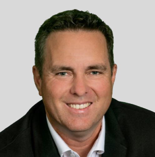
Todd Foulds
AMD
Todd Foulds is the Corporate Vice President of Product Engineering Operations at AMD with nearly 30 years of experience in the semiconductor industry. His team’s responsibilities cover Product Management, Product & Test engineering, Hardware & Infrastructure development, and Engineering Lab operations. Prior to joining AMD, Todd was a technical consultant at Hewlett Packard/Agilent Technologies in the ATE Test & Measurement division. Todd holds a Bachelor of Science degree in Electrical Engineering from Texas A&M University.
Company Profile
For 50 years, AMD has driven in high-performance computing, graphics, and visualization technologies – the building blocks for gaming, immersive platforms, and the datacenter. Hundreds of millions of consumers, leading Fortune 500 businesses and cutting-edge scientific research facilities around the world rely on AMD technology daily to improve how they live, work and play. AMD employees around the world are focused on building great products that push the boundaries of what is possible. For more information about how AMD is enabling today and inspiring tomorrow, visit AMD (NASDAQ:AMD) on their website, blog, Facebook and Twitter pages.


Panelist
Mike Slessor, Ph.D.
FormFactor
Michael D. Slessor has served as our Chief Executive Officer of FormFactor, Inc. since 2014, and as a Director since 2013. Mike served as President from 2013 to 2014, and as Senior Vice President and General Manager, MicroProbe Product Group from 2012 to 2013. Before joining FormFactor, he was President and Chief Executive Officer of MicroProbe from 2008 through the 2012 closing of FormFactor’s acquisition of MicroProbe. Prior to joining MicroProbe, he held various management, product-marketing, and applications-engineering positions in the semiconductor industry, primarily with KLA.
Mike received his Ph.D. in Aeronautics and Physics from the California Institute of Technology and his B.A.Sc. in Engineering Physics from the University of British Columbia.
Company Profile
FormFactor is a leading provider of essential test and measurement technologies along the full IC life cycle – from characterization, modeling, reliability, and design debug, to qualification and production test. Semiconductor companies rely upon FormFactor’s products and services to accelerate profitability.
FormFactor’s leading-edge probe stations, probes, probe cards, advanced thermal subsystems, quantum cryogenic systems and integrated systems deliver precision accuracy and superior performance both in the lab and during production manufacturing.
Visit www.formfactor.com or follow us on LinkedIn.


Panelist
Roy Chorev
Teradyne
Roy Chorev is the vice president of product development for the semiconductor test division at Teradyne, where he is responsible for product development for Teradyne’s semiconductor test products. With more than twenty years of experience in the automated test equipment industry, he has held a number of roles in software development, systems engineering and product marketing at Teradyne. Roy holds a Bachelor of Arts in computer science from McGill University and Master of Business Administration from Babson College.
Company Profile
Teradyne (NASDAQ:TER) brings high-quality innovations such as smart devices, life-saving medical equipment and data storage systems to market, faster. Its advanced test solutions for semiconductors, electronic systems, wireless devices and more ensure that products perform as they were designed. They solve complex test and automation challenges and enable businesses to achieve higher production volumes, higher quality and higher ROI. Its Industrial Automation offerings include collaborative and mobile robots that help manufacturers of all sizes improve productivity and lower costs. In 2021, Teradyne had revenue of $3.7 billion and today employs over 6,500 people worldwide. For more information, visit teradyne.com.
Corporate Headquarters
+1 978-370-2700
Contact Us
www.teradyne.com
Company Products & Services
Teradyne delivers manufacturing automation across industries, applications and the world. Teradyne solves complex test and automation challenges and enables businesses to achieve higher production volumes, higher quality and higher ROI. Teradyne designs, develops, and manufactures automatic test equipment used to test semiconductors, wireless products, data storage and complex electronics systems in a number of industries, including consumer electronics, wireless, automotive, industrial, computing, communications, and aerospace and defense. The industrial automation portfolio includes collaborative robotic arms, autonomous mobile robots (“AMRs”) and advanced robotic control software used by global manufacturing, logistics and industrial customers to improve quality, increase manufacturing and material handling efficiency, and decrease manufacturing and logistics costs. The automatic test equipment products include:

Panelist
Tessolve
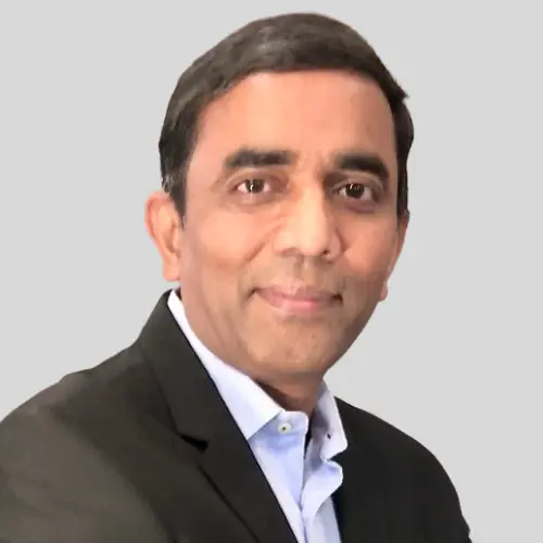
Srini Chinamilli is the Co-founder and CEO of Tessolve. He has more than 25 years of experience in semiconductor Test and Product engineering and held management and technical positions at Cirrus Logic and Centillium communications prior to co-founding Tessolve. Under his leadership, Tessolve has evolved to be the largest standalone semiconductor engineering solutions company, with over 3200 employees across 10 countries worldwide.
Company Profile
Tessolve is a leading semiconductor & systems engineering services company founded in 2004. With a global presence and over 3,200 employees, they support major technology companies. Tessolve offers a wide range of services including ASIC design, chip design, test engineering, complex PCB design, and embedded systems design. Their focus on emerging areas like AI, hyperscalars, semiconductor design and testing, avionics and automotive solutions helps clients bring high-quality products to market faster and more cost-effectively.
Panelist
Samer Kabbani
AEM Holdings
With decades of experience in the semiconductor capital equipment industry, Samer has extensive experience in leading technology M&A, R&D, business strategies development, implementation, and competitive strategy. He excels in product innovation and development that is designed to align to both market and customer requirements.
Before joining AEM, Samer was the Executive Vice President at Advantest and Astronics Test Systems. In his 14-year tenure at Cohu, Samer served in senior management roles, including Delta Design Systems president.
Samer is a prolific innovator with 30+ registered patents in areas of advanced thermal management, photoresist processing, factory automation, and vision alignment and inspection.
Company Profile
AEM: Unleashing the Power of Tomorrow – Leader in High-Performance Processor Testing for the AI Era
AEM is a global leader in intelligent system test and handling solutions for semiconductor and electronics companies serving the advanced computing, 5G, and AI markets. Our mission is to provide the most comprehensive semiconductor and electronics test solutions based on the best-in-class technologies, processes, and customer support.
AEM is the pioneer of massively parallel, fully automated test solutions. Our expertise has been developed over the past two decades where AEM now has the largest fleet of such high parallel systems in the world serving the advanced performance compute market.
AEM has a global presence across Asia, Europe, and the Americas, with R&D centers located in Singapore, Malaysia, France, Finland and the US. AEM has manufacturing plants in Singapore, Malaysia (Penang), Indonesia (Batam), Vietnam (Ho Chi Minh City), and Finland (Lieto), and a global network of field engineering support and sales offices.
Company Products & Services
AEM: Unleashing the Power of Tomorrow – Leader in High-Performance Processor Testing for the AI Era
AEM is a global leader in intelligent system test and handling solutions for semiconductor and electronics companies serving the advanced computing, 5G, and AI markets.
AEM’s technology pillars stem from the substantial investments made in R&D to sustain our leadership in three critical verticals: Industry leading Active Thermal Control, Advanced Factory Automation, and Application-Optimized Test Instrumentation.
AEM’s Solutions:
Industry Leading Active Thermal Control: Common active thermal collaterals integrated into various test insertion solutions ranging from the engineering lab to high volume manufacturing to enable rapid time to market and yield improvements.
Advanced Factory Automation: Factory 4.0 automation for low to massively parallel test insertions optimized for maximum throughput and lowest cost of test.
Test Instrumentation: Highly optimized test instrumentation, coupled with active thermal control and automation, that challenges the current cost-prohibitive traditional ATE test methodology.

17:45 – 18:15
Drive to Sharon Heights Golf Club
(17:45 Bus Departure at Plug and Play)
18:15 – 19:40
Cocktail
19:10 – 19:20

Christine Dunbar
Christine Dunbar formerly Head of Strategic Business Development at Natcast, the non-profit entity designated by the U.S. Department of Commerce to operate the National Semiconductor Technology Center (NSTC). In this role, she leads strategic initiatives to advance the U.S. semiconductor ecosystem, fostering collaboration between industry, government, and academia.
Before joining Natcast in March 2025, Christine served as Senior Vice President of Global Sales at IQE, a leading provider of compound semiconductor wafer products and advanced materials solutions. Prior to joining IQE in 2022, she held key executive roles at GlobalFoundries and IBM’s Microelectronics Division.
A Cornell University graduate with a bachelor’s degree in Materials Science and Engineering, Christine has dedicated her entire career to advancing the global semiconductor industry. In recognition of her leadership, she was nominated for the Global Semiconductor Association’s inaugural “Rising Woman of Influence” award in 2018.
Beyond her executive roles, Christine is a recognized thought leader and sought-after speaker on the critical issues shaping the future of the semiconductor industry. She is frequently called upon to present at global industry forums, where she has provided insights on technology innovation, supply chain resilience, workforce development, and global policy. A longtime advocate for diversity in tech, she is also deeply committed to mentoring and inspiring the next generation of leaders, helping to shape a more inclusive and dynamic semiconductor ecosystem.
19:40 – 22:30
Gala Dinner – Sponsored by TEL US
Welcome Dinner Speaker

Ben Rathsack, Ph.D.
Tokyo Electron
Ben Rathsack is Vice President of 2 US Business Units within Tokyo Electron America (TEA). He is responsible for the US business management (P/L) of the lithography track/ cleaning system BU (CTSPS) and assembly (3DI)/ test systems BU (ATS) including sales, marketing and service within the US. These business units drive advanced FEOL scaling and BEOL advanced packaging equipment sales. He has worked at TEA for 17 years in various roles including VP of Product and Technology Development (R&D), marketing, new product introduction and process development. He has 23 years of semiconductor experience at Tokyo Electron and Texas Instruments (50 publications/ 30 patents). He received his BS in Chemical Engineering from the University of Illinois/UC and his MS/PhD at the University of Texas/Austin.
Company Profile
As a leading global company of semiconductor and flat panel display (FPD) production equipment, Tokyo Electron Limited (TEL) engages in development, manufacturing, and sales in a wide range of product fields. Building on the technological expertise and know-how that we have been cultivating since our inception over 50 years ago, we strive to contribute to the development of a dream-inspiring society. All of TEL’s semiconductor and FPD production equipment product lines maintain high market shares in their respective global segments. TEL provides outstanding products and services to customers through a global network in the U.S., Europe, and Asia.
Website: https://www.tel.com/
Phone: +1-512-424-100
Additional Contact Information: https://www.tel.com/contactus/

22:30 – 23:00
Drive to Santa Clara Marriott
(22:30 Bus Departure at Sharon Heights Golf Club )
End of content
End of content