9-11 December 2025
Muscat, Oman
No posts
15-16 April 2025 - Silicon Valley


07:30 – 08:30
Registration
08:30 – 08:50
M.S.W.S., I.S.I.G. and P&P Welcome

Salah Nasri
International Semiconductor Industry Group (ISIG)
Salah Nasri is the CEO and Co-Founder of the International Semiconductor Industry Group (ISIG), a global organization founded in 2010 that connects and empowers semiconductor decision-makers through strategic leadership platforms, executive summits, and collaborative initiatives. ISIG has become a trusted global hub for industry leaders driving innovation and progress across the semiconductor value chain.
With extensive experience across the semiconductor sector, Salah has played a pivotal role in fostering global collaboration among industry leaders. Under his leadership, ISIG has evolved into one of the most influential communities in the semiconductor ecosystem—bringing together executives, innovators, and policymakers across regions including the United States, Europe, Asia, and the Middle East.
Salah has been instrumental in expanding ISIG’s reach and impact, curating high-level summits and initiatives that drive dialogue and progress across critical areas such as semiconductor manufacturing, AI, MEMS, automotive electronics, and advanced packaging. His vision continues to position ISIG as a key platform for thought leadership, networking, and strategic industry alignment.
Earlier in his career, Salah held positions at Credit Suisse, Goldman Sachs, Worldwide Business Research, and the International Business Development Group. He studied International Relations and Economics at Oxford University and Loughborough University, and in 2024 became a Stanford University alumnus after completing the Stanford Executive Program. In addition to his role at ISIG, Salah also serves on the Advisory Board of Atlant3D, a pioneer in atomic-layer advanced manufacturing solutions.
Company Profile
Established in 2010, the International SemiconductorIndustry (I.S.I.G.) is a prestigious & trusted associationwithin the semiconductor industry, renowned fororchestrating major regional summits across the globe,ranging from the U.S, the Middle East & Asia via ourdivision, the International Semiconductor ExecutiveSummits (I.S.E.S.). Our summits are fully endorsed bylocal governments and leading companies in all areas ofthe semiconductor supply chain.
Moreover, I.S.E.S. serves as the Premier platform for senior executives in technology, manufacturing, and R&D from diverse semiconductor companies, technology providers, and affiliated industries.
Our events are instrumental helping to shed light onto key industry trends, drive innovation and influence key decisions to help shape, and advance the growth of the semiconductor sector.


Saeed Amidi
Plug and Play Tech Center
Saeed is a seasoned investor and executive with over 30 years of experience growing businesses in numerous industries, including real estate, bottled water, packaging, and technology investing. Following the early success of his various businesses, The Amidi Group initially purchased a building in Palo Alto and decided to rent the extra office spaces to startups.
As the CEO and founder of Plug and Play, Saeed applies his passion for the tech industry daily by working with forward-thinking partners and the best global startups to facilitate positive change worldwide. Since Plug and Play’s launch in 2006, the company has worked with over 90,000 startups, made over 2,000 investments, and boasts over 30 unicorns including Dropbox, PayPal, Lending Club, N26, and Honey. Similar to his unexpected success with the “Lucky Building,” Saeed considered himself lucky overall when he moved to Silicon Valley in the late 70s, where he was then unaware of the ecosystem it would become.
Company Profile
Plug and Play is the ultimate innovation platform. Our mission is to build the world’s leading innovation platform and make innovation open to anyone, anywhere. We do this by connecting entrepreneurs, corporations, and investors worldwide.
Over the past 15 years, we have brought together 35,000+ startups, 500+ world-leading corporations, and hundreds of venture capital firms, universities, and government agencies across 20+ industries.
We are active in 50+ locations globally, including the U.S., China, France, Germany, South Africa, Singapore, Indonesia, Brazil, and more.
Together with our partners, we are creating a unique ecosystem designed to facilitate meaningful introductions, invest in startups, and bring together key stakeholders.
The industries we focus on include Agtech, Animal Health, Brand & Retail, Crypto & Digital Assets, Energy, Enterprise, Fintech, Food & Beverage, Health, Insurtech, IoT, Maritime, Media & Ad, Mobility, New Materials & Packaging, Real Estate & Construction, Smart Cities, Supply Chain, Sustainability, and Travel & Hospitality.


Rouzbeh Borhani
Plug and Play Tech Center
Rouzbeh is the Founder and Head of the Semiconductor practice at Plug and Play, the largest corporate innovation platform in the world and one of the most active early-stage investors globally. He collaborates closely with entrepreneurs, corporate innovation leaders, and investors, focusing on the semiconductor industry value chain.
Previously, Rouzbeh served as the Country Retail Management Director in the Consumer Electronics sector.
Rouzbeh holds a Master of Business Administration and a Master of Science in Disruptive Innovation, along with a Bachelor of Science in Mechatronics Engineering. He is currently a PhD candidate in Electrical and Computer Engineering. His passion lies at the intersection of technology and business.
Company Profile
Plug and Play is the ultimate innovation platform. Our mission is to build the world’s leading innovation platform and make innovation open to anyone, anywhere. We do this by connecting entrepreneurs, corporations, and investors worldwide.
Over the past 15 years, we have brought together 35,000+ startups, 500+ world-leading corporations, and hundreds of venture capital firms, universities, and government agencies across 20+ industries.
We are active in 50+ locations globally, including the U.S., China, France, Germany, South Africa, Singapore, Indonesia, Brazil, and more.
Together with our partners, we are creating a unique ecosystem designed to facilitate meaningful introductions, invest in startups, and bring together key stakeholders.
The industries we focus on include Agtech, Animal Health, Brand & Retail, Crypto & Digital Assets, Energy, Enterprise, Fintech, Food & Beverage, Health, Insurtech, IoT, Maritime, Media & Ad, Mobility, New Materials & Packaging, Real Estate & Construction, Smart Cities, Supply Chain, Sustainability, and Travel & Hospitality.


Rouzbeh Borhani
Plug and Play Tech Center
Rouzbeh is the Founder and Head of the Semiconductor practice at Plug and Play, the largest corporate innovation platform in the world and one of the most active early-stage investors globally. He collaborates closely with entrepreneurs, corporate innovation leaders, and investors, focusing on the semiconductor industry value chain.
Previously, Rouzbeh served as the Country Retail Management Director in the Consumer Electronics sector.
Rouzbeh holds a Master of Business Administration and a Master of Science in Disruptive Innovation, along with a Bachelor of Science in Mechatronics Engineering. He is currently a PhD candidate in Electrical and Computer Engineering. His passion lies at the intersection of technology and business.
Company Profile
Plug and Play is the ultimate innovation platform. Our mission is to build the world’s leading innovation platform and make innovation open to anyone, anywhere. We do this by connecting entrepreneurs, corporations, and investors worldwide.
Over the past 15 years, we have brought together 35,000+ startups, 500+ world-leading corporations, and hundreds of venture capital firms, universities, and government agencies across 20+ industries.
We are active in 50+ locations globally, including the U.S., China, France, Germany, South Africa, Singapore, Indonesia, Brazil, and more.
Together with our partners, we are creating a unique ecosystem designed to facilitate meaningful introductions, invest in startups, and bring together key stakeholders.
The industries we focus on include Agtech, Animal Health, Brand & Retail, Crypto & Digital Assets, Energy, Enterprise, Fintech, Food & Beverage, Health, Insurtech, IoT, Maritime, Media & Ad, Mobility, New Materials & Packaging, Real Estate & Construction, Smart Cities, Supply Chain, Sustainability, and Travel & Hospitality.

08:55 – 09:15
Keynote
Sensing Hope at the Edge
Machine Learning at THE EDGE. Nearly every company, investor, product launch, and presentation these days is about “ML at The Edge” as the next, great technology wave. And where there is a wave, there are riders, hoping to cash in. For me, sensors are clearly the edge, breaking the boundary between the physical and digital worlds. Driven by cost, size, power constraints, MEMS is the technology sensing the edge. And with so much data being collected, doing the analysis at the edge with ML decreases latency and saves power on data transmission. But where is the money? I’ll talk about the forces at play, large and small, and offer some experiences from MEMS at the edge. And also share my hope that beyond the hype, there is good to be done. That new understanding from all the data and algorithms will help us to leave the planet better than we found it.

Peter Hartwell, Ph.D.
TDK InvenSense
Dr. Peter G. Hartwell is VP of Engineering at TDK US Corporation driving global technology and strategy. Peter came to TDK through its acquisition of Invensense where he was the CTO. Peter has over 30 years experience commercializing silicon MEMS systems, working on sensors, actuators, and software at all levels. Prior to InvenSense, Peter was Architect of Sensing Hardware at Apple and was a Distinguished Technologist at Hewlett-Packard Labs. Peter has over 40 worldwide patents on MEMS devices and sensor applications. Peter has a B.S. in Materials Science from the University of Michigan and a Ph. D. in Electrical Engineering from Cornell University.
Company Profile
InvenSense, a TDK Group company, is a world-leading provider of sensor solutions, including MEMS and magnetic sensors for consumer, industrial, and automotive applications. InvenSense MEMS sensors are known to be best-in-class for reasons that include high performance and reliability, high-volume manufacturing capacity and supply stability, ongoing hardware and software innovation, and ultra-low power consumption. They can be found in Mobile, Wearable, Smart Home, Industrial, Automotive, IoT, and Robotics products, among others. Founded in 2003, InvenSense has a 20+ year history of patented sensor technology across Motion, Sound, and Ultrasonic solutions, including the invention of the 6-axis IMU. InvenSense is dedicated to enabling partner success and enhancing lives through sustainable sensor innovation. In May of 2017, InvenSense became part of the MEMS Sensors Business Group of TDK Corporation, based in Tokyo, Japan. InvenSense is headquartered in San Jose, California and has offices in Boston, China, Taiwan, Korea, Japan, France, Canada, Slovakia, and Italy.

09:20 – 09:40
Keynote
Sensors and Systems in an AI first world
It seems that everything today is an AI first device, but what does this mean? In this talk I will discuss some of the ways that AI is impacting how Google thinks about our hardware devices and the components within. I will talk through some of the growing systems level considerations for number of sensors, quality and precision of measurements as well as how compute is distributed to handle the various AI models that exist. The goal will be to give the audience an overview of what exists today as well as some possibilities of how they can help shape devices of tomorrow.

Michael Pate, Ph.D.
Dr. Michael Pate received advanced degrees from Texas Tech University and Denmark Technical University concentrating in the design of Class-D amplifiers for audio systems. After completing his Ph.D. work he began at Texas Instruments where he led the design of some of the highest power integrated Class-D amps on the market. From there Dr Pate moved to product definition roles at Cirrus Logic, Audience and Knowles Electronics where he focused on mixed signal audio, DSP and algorithms and MEMS microphones respectively. He now works at Google as the Director of Audio Technology Development where his team builds experiences like Active Noise Cancellation, Audio Magic Eraser, Clear Calling and many more.
Company Profile
A problem isn’t truly solved until it’s solved for all. Googlers build products that help create opportunities for everyone, whether down the street or across the globe. Bring your insight, imagination and a healthy disregard for the impossible. Bring everything that makes you unique. Together, we can build for everyone.

09:45 – 10:45
Networking Break and Business Meetings
10:50 – 11:10
Enhancing human perception – sensors of the future as extensions of our five senses
Sensors have always enabled new ways of interacting with the world that surrounds us. By enhancing our natural abilities to see, hear, taste, smell and touch, they are a natural extension of our 5 senses. Thanks to the rapid advances of AI, we will soon be able to experience a new level of personalization, assistance and support through sensor-enabled devices, touching all aspects of our lives.
Developing and producing high-performance sensors which are secure, sustainable, affordable and easy to use is our mission at ST. Aligned with our mission, the speech will showcase examples of sensor-driven innovation in several applications like wearables, vital sign monitoring, mobility and robotics.

Anton Hofmeister
STMicroelectronics
Anton Hofmeister is Group Vice President and General Manager of R&D in ST’s Analog, Power & Discrete, MEMS & Sensors Group. He is also Managing Director of ST’s German subsidiary since 2016.
Hofmeister joined Thomson Semiconductors (a predecessor company to STMicroelectronics) as a marketing engineer in 1986. He subsequently held management positions in product marketing, key account management and corporate strategic marketing. In 1997, Hofmeister was appointed Director of a System R&D team in San Diego, USA, and became subsequently Director of the Print Head Business Unit. In 2005, he was appointed General Manager of the Microfluidics Division and has broadened his responsibility with the MEMS Microactuator Division in 2015, managing the MEMS business for a variety of applications in Consumer Electronics, Automotive, Industrial, and Medical markets.
Hofmeister has served as a board member of the Singapore-based Molecular Diagnostics company Veredus Laboratories. He is currently a member of the Governing Council of the MEMS&Sensor Industry Group (MSIG) at SEMI and a board member of the European Association on Smart Systems Integration (EPoSS).
Anton Hofmeister was born in Munich and graduated with a Master’s degree in Engineering from the University of Munich.
Company Profile
At ST, we are more than 50,000 creators and makers of semiconductor technologies mastering the semiconductor supply chain with state-of-the-art manufacturing facilities. An integrated device manufacturer, we work with more than 200,000 customers and thousands of partners to design and build products, solutions, and ecosystems that address their challenges and opportunities, and the need to support a more sustainable world. Our technologies enable smarter mobility, more efficient power and energy management, and the wide-scale deployment of cloud-connected autonomous things. We are committed to achieving our goal to become carbon neutral on scope 1 and 2 and partially scope 3 by 2027. Further information can be found at www.st.com.

11:15 – 11:35
Understanding “who spoke when?”: High SNR MEMS Microphones and the Evolution of AI Understanding
Better audio input is essential for making AI suitable for everyday use. In noisy environments, AI can more easily recognize different speakers in a conversation if audio is recorded with high SNR (Signal-to-Noise Ratio) MEMS microphones. Improving audio input reduces misunderstandings and enhances the quality of translations. AI applications using high SNR MEMS microphones revolutionize how devices interact with the world by enabling advanced environment recognition, speaker recognition and sound classification.

Roberto Condorelli
Infineon Technologies AG
Roberto is a high-tech industry veteran with 20+ years of experience driving disruptive technologies in the semiconductor sector. Roberto’s expertise spanning manufacturing, marketing, and business development. Passionate about staying at the forefront of industry trends and advancements Roberto recently dedicated his focus on IoT and Audio applications requiring unprecedent High SNR MEMS Microphones. Roberto and his team are concentrating on high-fidelity voice call on-the-go, immersive sound and natural human interaction with AI-machine applications. Roberto’s expertise bridges technical innovation and customer-centric solutions.
Company Profile
Here at Infineon, we combine entrepreneurial success with responsible action to make life easier, safer, and greener. Barely visible, semiconductors have become an indispensable part of everyday life. We play a key role in shaping a better future – with microelectronics that link the real and the digital world. Our semiconductors enable efficient energy management, smart mobility, as well as secure, seamless communications in an increasingly connected world. Infineon designs, develops, manufactures and markets a broad range of semiconductors and system solutions. The focus of its activities is on automotive and industrial electronics, communication and information technologies, IoT, sensor technology and security. The product range comprises standard components, software, customer-specific solutions for devices and systems, as well as specific components for digital, analog, and mixed-signal applications.

11:40 – 12:00
Monolithic CMOS-MEMS Foundry Convergence: Unlocking the Future of Piezoelectric Sensors and Emerging Technologies
The convergence of monolithic CMOS and MEMS foundries is paving the way for the next generation of sensor technologies, particularly in the realm of piezoelectric devices. This integration allows for the seamless coupling of advanced semiconductor fabrication with MEMS structures, enabling ultra-compact, high-performance piezoelectric sensors. The emergence of chiplet-based architectures further enhances design flexibility, reducing costs, and accelerating time-to-market. This presentation will explore how this convergence supports the development of cutting-edge technologies, ranging from advanced wearables to medical devices, and its implications for the future of sensor-driven applications across industries.

Eloi Marigo, Ph.D.
SilTerra
ELOI MARIGO was born in Barcelona, Spain, in 1985. He received the degree in Engineer Telecommunications, a Master in Micro and Nanoelectronics and a Ph.D. degree in electrical engineering from Universitat Autònoma de Barcelona, Bellaterra, Spain, in 2008, 2009 and 2012 respectively. In 2013, he joined the Department of Technology Development, Silterra Malaysia Sdn. Bhd., as a Senior Engineer, and in 2024 he became a Senior Manager. His current research interests include the design, simulation, fabrication and characterization of monolithic CMOS-MEMS with special focus on piezoelectric devices.
Company Profile
SilTerra, a pure-play wafer foundry, offers various CMOS technologies from 180nm to 110nm nodes. It serves a wide range of end-market applications, including IoT, power management, consumer electronics, medical and communication products. Besides CMOS technologies, SilTerra also provides MEMS foundry services, unique and patented MEMS-on-CMOS technologies, silicon photonics, bio-photonics, and power. Its excellent customer service team helps customers realize working prototypes from proof of concept to high volume manufacturing.

12:05 – 13:05
Buffet Lunch
13:10 – 13:30
From an Idea to a Sensor Product: Micro Needle Case Study
What all is needed to fabricate a new sensor component, using microneedles as a case study. Raw concept idea, expected specifications, defining the uncertainties, when to include the foundry. Collaboration is vital to identify the unknowns in function and fabrication and to prepare needed design variants to derisk the prototypes and achieve informative results as early as possible. And with first results come specification refinement, what should the end function really be? Learning through a biomedical micro needle implant project.

Jared Crawford
Teledyne MEMS
With over 20 years of experience in MEMS research and development, Jared has played a pivotal role in advancing microfabrication technologies. His expertise spans process design, prototype development, and transfer of innovations to manufacturing. As a technical expert, he specializes in developing foundational building blocks tailored to projects with unique requirements including optical switches, RF switches, microphones, and microfluidics.
Jared conducts technical assessments and process designs for emerging opportunities, leveraging his deep knowledge of MEMS fabrication techniques. He has been instrumental in bringing biomedical implant products from prototype through to human trials, ensuring that cutting-edge MEMS products make a real-world impact in healthcare.
Company Profile
Teledyne MEMS is an industry-leading pure-play MEMS foundry, specializing in manufacturing MEMS and microfabrication solutions, from initial prototypes to high-volume production, across two Canadian sites.
Our commitment lies in maintaining stringent quality systems, delivering exceptional service, and safeguarding customer intellectual property. We take pride in our track record of transitioning customer designs to mass production with efficiency and precision. Partnering with us means gaining access to extensive technical expertise and advanced fabrication capabilities, ensuring that we add value to your projects through our experience.
With decades of experience, we produce devices for diverse markets including micro-mirrors for telecommunications, gyro sensors for game controllers, microfluidic devices for miniaturized medical systems, and inertial sensors for automobiles. Our innovative MEMS enhance performance while reducing size and power consumption.

13:35 – 13:55
Advancements in Silicon Photonics Through Heterogeneous Integration
Heterogeneous Integration (HI) is critical to silicon photonics as new materials improve specifications. HI supports advances in , telecom, quantum computing, AI, AR/VR and biomedical sensors. X-FAB will act as an open foundry offering a modular integration architecture for lasers, modulators and photodetectors using its 200mm MEMS toolset.

Stefan Ernst, Ph.D.
X-FAB
Stefan studied physics in Dresden, Germany, and Edinburgh, UK. He obtained his PhD in the field of low-temperature solid state physics. Since joining X-FAB in 2011, he worked in various positions in technology development, engineering and program management. In his current role as Marketing Director, Stefan overlooks the global Business Development for MEMS and Microsystems Technologies at the X-FAB Foundry Group.
Company Profile
X-FAB is one of the world’s leading specialty foundry groups for analog/mixed-signal semiconductor technologies with a clear focus on automotive, industrial, and medical applications. As a pure-play foundry, X-FAB provides manufacturing and design support services to customers that design analog/mixed-signal integrated circuits (ICs) and other semiconductor devices for use in their own products or the products of their customers. Its customers worldwide benefit from the highest quality standards, manufacturing excellence and innovative solutions by using X-FAB’s modular CMOS and SOI processes in geometries ranging from 1.0 µm to 110 nm, and its special micro-electro-mechanical systems (MEMS) processes. X-FAB is also the first pure-play foundry to provide comprehensive processing technologies for the wide-bandgap materials silicon carbide (SiC) and gallium nitride (GaN). The GaN-on-Si wafers are manufactured in its modern 8” fab in Dresden, Germany, and SiC wafers in the 6” fab in Lubbock, Texas, USA. X-FAB runs six production facilities in Germany, France, Malaysia and the U.S. The company employs about 4,200 people worldwide.

14:00 – 14:10
The Future of Atomic Layer Advanced Manufacturing
ATLANT 3D is pioneering a new era of atomic-scale manufacturing, enabling the creation of materials and devices with unprecedented precision. Our patented Direct Atomic Layer Processing (DALP®) technology redefines microfabrication, bridging the gap from lab to fab. With our NANOFABRICATOR™ platform, research teams and industries can develop next-generation quantum, semiconductor, advanced packaging, MEMS/sensors and space technologies faster and more efficiently. By replacing complex, resource-intensive processes with precise atomic-scale fabrication, we empower innovators to build the technologies of tomorrow while driving sustainability. Join us to explore how atomic control is unlocking new possibilities for advanced manufacturing and scientific breakthroughs.

Bonnie Tsim, Ph.D.
ATLANT 3D
Dr. Bonnie Tsim is Head of Strategic Initiatives at ATLANT 3D and holds a PhD in Theoretical Physics on the electronic properties of twistronic graphene from the University of Manchester. With expertise across deep-tech strategy, advanced materials, and international ecosystem building, she has led AI strategy and digital transformation at Turner & Townsend and convened global stakeholders in exponential technologies such as quantum and semiconductors at MATTER.
Company Profile
ATLANT 3D has mastered control of matter at the atomic scale, ushering in a new era in manufacturing. For research teams and manufacturers working at the frontiers of technology, we’ve created what was once thought unattainable: a system that builds materials and devices, atom by atom, with unprecedented precision and speed.
While others are constrained by traditional manufacturing limits, our breakthrough technology makes it possible to create the seemingly impossible, from next-generation quantum computers to devices that can operate in the harsh conditions of space. By replacing complex, resource-heavy processes with precise atomic-scale fabrication, we’re transforming technology while making manufacturing sustainable. We’re providing innovative teams the power to build technologies today that will define tomorrow’s world, using fewer resources to achieve greater possibilities.
Based in Copenhagen and London, with operations in the US, ATLANT 3D partners with research institutions and industrial companies to expand the boundaries of technological possibility.
Company Products & Services
ATLANT 3D is redefining microfabrication with its patented Direct Atomic Layer Processing (DALP®) technology. Our NANOFABRICATOR™ platform enables localized atomic layer processing for rapid material discovery, prototyping, and scalable device fabrication—bridging the gap from lab to fab.
Beyond hardware, we offer Pilot Projects and Joint Development Services to validate new materials and device architectures. A-HUB, our Microfabrication-as-a-Service (MaaS) centre, provides R&D teams with atomic-scale precision without the need for costly infrastructure.
From concept to fabrication, ATLANT 3D partners with academia and industry to drive next-generation innovations beyond conventional limits.

14:15 – 14:25
MEMS at the crossroads of innovation – Converging with emerging technologies
What if the smallest microsystem could unlock the biggest technological breakthroughs?! MEMS have already revolutionized countless sectors, but their true potential is only beginning to unfold. At Silicon Austria Labs (SAL), we are looking at MEMS converging with photonics, magnetics, AI and even quantum technologies—pushing the boundaries of precision, speed, and intelligence. The future of transduction isn’t just about miniaturization – it’s about pioneering intelligent, hyper-connected ecosystems that will transform industries in ways we never imagined. Join us for a glimpse into SAL unfolding the future!
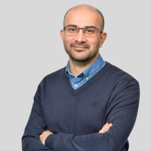
Mohssen Moridi, Ph.D.
Silicon Austria Labs (SAL)
Dr. Mohssen Moridi is an expert in microtechnology with over 20 years of experience in the development of MEMS devices. He holds a Master’s and Ph.D. in Microtechnology from École Polytechnique Fédérale de Lausanne (EPFL), Switzerland. After completing his doctoral studies, he held various research positions in Switzerland, contributing to advancements in microsystems technology. In 2016, he moved to Austria to lead the Microsystem Division at CTR AG, where he established a MEMS department and managed the development of a new cleanroom dedicated to industrial R&D. Since 2019, he has been part of Silicon Austria Labs (SAL) and currently serves as Senior Executive Director and Head of the Microsystems Research Division. In this role, he leads a team of over 60 researchers, driving innovation in thin-film technologies, integrated photonics, and magnetic and piezoelectric microsystems. With extensive experience at the intersection of research and industry, Dr. Moridi plays a key role in shaping cutting-edge microsystem technologies, bridging fundamental research with industrial applications.
Company Profile
Silicon Austria Labs (SAL) has been founded to be a top European research center for electronic-based systems. In the network of science and economy, we carry out research at a global level and create the basis of groundbreaking products and processes.

14:30 – 14:50
APECS Research Pilot Line for advanced heterointegration innovations in the MEMS Industry
The pilot line for “Advanced Packaging and Heterogeneous Integration for Electronic Components and Systems” (APECS), funded by the EU Chips Act, advances Europe’s semiconductor manufacturing and chiplet innovation. With €730 million over 4.5 years, it enhances EU technological resilience by bridging application-oriented research with innovative chiplet technologies. APECS focuses on chiplet system design for computing, AI, and MEMS sensors/actuators, using 3D stacking, 2.5D wafer-level integration, and quasi-monolithic integration. It aims to be Europe’s hub for advanced packaging, fostering collaboration among RTOs, industry, and academia to accelerate progress from research to scalable manufacturing.
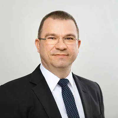
Jörg Amelung
Fraunhofer Institute for Photonic Microsystems
Jörg Amelung is Deputy Director of the Fraunhofer Institute for Photonic Microsystems (IPMS) and heads the MEMS Engineering, Manufacturing & Test division. Fraunhofer IPMS is a leading research institute in the MEMS field, equipped with high quality microsystem cleanrooms (200 – 300 mm wafer). As an expert and manager in MEMS technology, Jörg Amelung has been driving the development of smart microsystem technologies since 1993. He also played a key role in OLED development and founded two companies specializing in this field.
Company Profile
Fraunhofer IPMS is a leading international research and development service provider for electronic and photonic microsystems in the application fields of Smart Industrial Solutions, Bio and Health, Mobility as well as Green and Sustainable Microelectronics. Research focuses on customer-specific miniaturized sensors and actuators, MEMS systems, microdisplays and integrated circuits as well as wireless and wired data communication, neuromorphic and quantum computing. Services range from consulting and design to process development and pilot series production.
The Fraunhofer IPMS is one of 75 institutes of the Fraunhofer-Gesellschaft, the leading organization for applied research in Europe. With nearly 32,000 employees Fraunhofer operates with an annual budget of €3.6 billion, €3.1 billion of which is generated by contract research — Fraunhofer’s core business model.
Company Products & Services
The range of services includes wafer processing, characterization & testing, assembly and interconnection technology and the organization of external and supplier services. At the Center Nanoelectronic Technologies (CNT), Fraunhofer IPMS offers applied research, process and material development on 300 mm wafers for microchip producers, suppliers, device manufacturers and R&D partners. 4000 m² of clean room space is available for processing customer orders as well as laboratory space for over 80 processing and analytical tools.

14:55 – 15:25
Networking Break
15:30 – 15:50
Unlocking the Unseen: Polarization Image Sensing for Consumer Electronics
A single metasurface, made of subwavelength nanostructures, can perform optical functions that traditionally require multiple refractive or diffractive optics. In addition to the cost, size, and complexity improvements they offer to existing sensing systems, their unique ability to capture polarized light information enables new sensing capabilities at unprecedented form factors. Metalenz is bringing never-before-accessed information to machine vision with Polar ID, the first complete system solution built around metasurface optics. It is a new way of image sensing for mobile and beyond, enabling new insights and use cases for machine vision systems and consumers.

Rob Devlin, Ph.D.
Metalenz
Rob Devlin is co-founder and CEO of Metalenz, the first company to commercialize metasurface technology for mass markets. He holds a BS/MS in Electrical Engineering and Materials Science from Drexel University and a Ph.D. in Applied Physics from Harvard University in the lab of Professor Federico Capasso. His research has spanned the topics of nanofabrication, nanophotonics, and materials science. In 2025, he was awarded Optica’s Kevin P Thompson Design Innovator Award for his critical contributions to foundational optical metasurface design, pioneering leadership to commercialize metasurface optics, and product development of the first polarization sensor for consumer markets. Leveraging the unique capabilities of metasurfaces to capture all information in light and be mass manufactured in existing semiconductor foundries, Rob and his team at Metalenz are bringing complex optical sensing systems to mobile form factors and price points for the first time.
Company Profile
Metalenz is at the forefront of driving innovation in optics with metasurface technology, providing solutions that redefine the possibilities of mobile imaging and sensing. As the first company to bring metasurface optics to mass markets, Metalenz’s meta-optic components shrink the size, complexity, and price point of existing sensing systems. Now, leveraging the unique abilities of metasurfaces, the company’s next-gen end-to-end image sensing solutions enable consumer devices to see beyond the limits of current visual systems, bringing powerful new insights to our lives.
Company Products & Services
Visit Company Website
15:55 – 16:15
The Seismic Patch for Cardiovascular and Pulmonary Monitoring and Diagnosis
The convergence of precision Micro-Electro-Mechanical Systems (MEMS) sensors and actuators and Artificial Intelligence (AI) is revolutionizing digital health, particularly in cardiopulmonary and vascular care. MEMS-based sensors enable continuous, real-time monitoring of physiological parameters by analyzing heart and lung sounds and vascular dynamics with high precision and minimal invasiveness. When combined with AI-driven analytics, these data streams provide deep insights into cardiovascular and pulmonary health, facilitating early disease detection, personalized interventions, and improved patient outcomes.
This talk introduces the SeismicTM Patch, a smart wearable device empowered by the integration of MEMS, CMOS and AI algorithms in a small size that provides longitudinal monitoring and interpretation of complex cardiovascular and pulmonary acoustic signals, enabling automated diagnostics, predictive modeling for patient-specific risk assessment, and decision support for clinicians.

Farrokh Ayazi, Ph.D.
StethX Microsystems
Farrokh Ayazi is the Founder and CEO of StethX Microsystems, a spin-off of the Georgia Tech Integrated MEMS Laboratory that is commercializing advanced wearable patches for cardiopulmonary applications. He received the B.S. degree from the University of Tehran, Iran, in 1994, and the M.S. and Ph.D. degrees from the University of Michigan, Ann Arbor, in 1997 and 2000, respectively, all in electrical engineering. Dr. Ayazi is the Regents Entrepreneur and Ken Byers Professor in Microsystems at the Georgia Institute of Technology, where his main research interest lies in the area of integrated Micro/Nano-Electro-Mechanical-Systems (MEMS and NEMS), with a focus on high-Q acoustic resonators and advanced inertial sensors. Dr. Ayazi was the co-founder and CTO of Qualtré, a spin-out of his research laboratory that commercialized bulk acoustic wave silicon gyroscopes for high precision applications, which was acquired by Panasonic in 2016. Dr. Ayazi is a fellow of the IEEE, has authored over 300 refereed technical and scientific articles, and holds more than 60 patents. He was the general chair of the IEEE Micro-Electro-Mechanical-Systems conference in 2014, held in San Francisco, CA.
Company Profile
StethX is a start-up company located in Atlanta, GA commercializing a proprietary wearable sensor technology that enables remote and long-term monitoring of cardio-pulmonary conditions with high fidelity.

16:20 – 16:30
The path to quantum sensor wafer level manufacturing
Scaling quantum sensors from lab prototypes to high-volume manufacturing requires bridging the gap between precision quantum physics and semiconductor fabrication. At Mesa Quantum, we are developing a wafer-level manufacturing process to enable cost-effective, chip-scale quantum sensors for Position, Navigation, and Timing (PNT) applications. This involves integrating quantum materials with CMOS-compatible techniques, optimizing vacuum packaging, and ensuring reproducibility at scale. Collaborating with MEMS foundries is critical to achieving the precision and scalability needed for commercial deployment. This talk will explore key challenges, process innovations, and the role of foundries in advancing quantum sensor manufacturing for real-world applications.

Sristy Agrawal, Ph.D.
Mesa Quantum Systems
Sristy Agrawal, PhD, is the CEO and co-founder of Mesa Quantum Systems, a company pioneering chip-scale quantum sensors for resilient Position, Navigation, and Timing (PNT) solutions. She earned her PhD in physics from the University of Colorado, Boulder, where she worked at JILA & NIST, specializing in quantum sensing.
Driven by the need for GPS-resilient communication & navigation, Sristy co-founded Mesa Quantum to bridge the gap between quantum research and scalable manufacturing. She has won multiple prestigious entrepreneurship competitions, including Harvard’s President Innovation Challenge and Rice Business Battle, and was recognized on the Forbes 30 Under 30 list for her contributions to quantum technology. A passionate advocate for deep-tech innovation and defense applications, she is committed to bringing high-performance quantum sensors into real-world deployment.
Company Profile
Mesa Quantum Systems is pioneering chip-scale quantum sensors to enable GPS-independent Position, Navigation, and Timing (PNT) solutions for defense, aerospace, and autonomous systems. Traditional navigation relies on GPS, which is vulnerable to jamming, spoofing, and signal loss in contested environments. Mesa Quantum’s miniaturized, high-precision low SWAP clocks provide resilient navigation and timing where GPS is unavailable or compromised.

16:35 – 17:15
Panel Session Fueling Innovation and Overcoming MEMS Adoption Challenges: A Path Forward

Moderator
Britta Aldejohann
TE Connectivity
Britta Aldejohann is a Principal R&D/Product Development Engineer at TE Connectivity, specializing in sensors for minimally invasive applications such as catheters and endoscopes. With over two decades of experience at TE, Britta has demonstrated technical expertise and leadership in the field of sensor technology and product development.
Britta’s journey at TE Connectivity began in 2003 when she joined as an intern. Over the years, she has held various technical and managerial roles, showcasing her versatility and commitment to innovation.
Britta holds a Dipl.-Ing. degree (equivalent to a Master of Science) in Electrical Engineering from the RWTH Aachen University in Germany.
Company Profile
TE Connectivity is a global industrial technology leader creating a safer, sustainable, productive, and connected future. Our broad range of connectivity and sensor solutions enable the distribution of power, signal and data to advance next-generation transportation, renewable energy, automated factories, data centers, medical technology and more. With more than 85,000 employees, including 9,000 engineers, working alongside customers in approximately 130 countries, TE ensures that EVERY CONNECTION COUNTS.


Panelist
Alissa M. Fitzgerald, Ph.D.
A.M. Fitzgerald & Associates, LLC
Dr. Fitzgerald has over 30 years of engineering experience in MEMS design and fabrication. Prior to founding AMFitzgerald, Dr. Fitzgerald worked in engineering and management positions at several high-tech companies. She received bachelor’s and master’s degrees from MIT and a Ph.D. from Stanford University in Aeronautics and Astronautics. She co-authored MEMS Product Development: From Concept to Commercialization. In 2013, she was inducted into the MEMS Industry Group Hall of Fame and in 2024, she was Sensors Converge Executive of the Year. She is a board director for Rigetti Computing (Nasdaq:RGTI) and the IEEE Spectrum Editorial Advisory Board.
Company Profile
Founded in 2003, AMFitzgerald has been a key development partner to over 200 clients around the world, ranging in size from startups to Fortune 100 companies. Our team of experts develops all types of MEMS sensors and actuators for applications in consumer electronics, medical devices, industrial, aerospace, and scientific markets. MEMS products designed and developed by AMFitzgerald are helping to save lives, improve quality and safety of life, and reduce waste and inefficiency in industrial processes. Our services range from technology strategy to design-prototype-test, and supply chain management. We can accelerate the ramp to volume using integrated design-for-foundry relationships for piezoresistive pressure sensors and PZT piezoelectric MEMS. We also help shape our customers’ business and product strategies by leveraging our deep technical knowledge and unique industry insight. We are well known in the MEMS industry for our technical expertise, practical approach to manufacturing, and forthright assessment of risk. Our customers trust us with their most critical projects and return to us year after year. Want to know more? Ask us at info@amfitzgerald.com.


Panelist
Marcellino Gemelli
Bosch Sensortec
Marcellino Gemelli received the ‘Laurea’ degree in Electronic Engineering at the University of Pavia, Italy while in the Italian Army and an MBA from MIP, the Milano (Italy) Polytechnic business school. He is currently based in Sunnyvale (CA) USA, responsible for business development of Bosch Sensortec’s MEMS product line. He is also an angel investor and advisor to tech startups. He previously held various engineering and product management positions at STMicroelectronics from 1995 to 2011 in the fields of MEMS, electronic design automation and data storage. He was contract professor for the Microelectronics course at the Milano (Italy) Polytechnic from 2000 to 2002.
Company Profile
Bosch Sensortec is a wholly owned subsidiary of the Bosch Group, dedicated to developing and marketing a comprehensive portfolio of microelectromechanical systems (MEMS)-based sensors and solutions for consumer electronics. Headquartered in Reutlingen, Germany, the company was founded in 2005 and has since become a global leader in MEMS sensor innovation. Bosch Sensortec’s product offerings include motion sensors, environmental sensors, smart sensors, and software solutions that power a wide range of devices such as smartphones, wearables, drones, and IoT applications.
By leveraging Bosch’s decades of experience and leadership in automotive MEMS sensor technology, Bosch Sensortec brings industrial-grade performance to the consumer market. With a focus on miniaturization, energy efficiency, and intelligent sensing, the company enables smart, connected devices that respond to their environments with precision and reliability. Through continuous innovation and a strong global network, Bosch Sensortec plays a pivotal role in advancing next-generation sensor technologies for an increasingly digital and mobile world.


Panelist
Martin Lim
xMEMS Labs
Martin Lim is currently VP of MEMS Technology at xMEMS. His role is to develop a piezoMEMS platform to support microspeakers and to develop ultrasonic air pulse technology which is the foundation for the next generation audio devices and the fan-in-chip air pumps for microcooling. Prior to xMEMS he was a co-founder of InvenSense where he established the CMOS-MEMS wafer bonding platform for inertial devices with wafer production rates exceeding 5000 wafers/month cumulative across multiple CMOS-MEMS foundries. Previously, he held key roles at Systron Donner Inertial, Sitek, and Xerox PARC, leading process integration for gyroscopes, pressure sensors, and acoustic MEMS. With multiple patents and publications, Martin has been instrumental in advancing MEMS process technologies for consumer electronics, automotive, and industrial applications worldwide.
Company Profile
Founded in January 2018, xMEMS Labs is the “X” factor in silicon MEMS with the world’s most innovative piezoMEMS platform. It began by delivering the world’s first solid-state True MEMS speakers for wireless earbuds and other personal audio devices. xMEMS’ “Sound from Ultrasound” technology delivers high-fidelity and full-bandwidth sound in a 1-mm thin package for earbuds, smart glasses, and smart watches.
xMEMS has evolved its ultrasonic piezoMEMS platform to also produce the world’s first μCooling fan-on-a-chip delivering critical active thermal management to smartphones, SSDs, XR and even isolated areas of datacenter rack servers underserved by conventional cooling technologies.
xMEMS has over 200 granted patents worldwide for its technology. For more information, visit https://xmems.com.
Company Products & Services


Panelist
InchFab
Mitchell Hsing is the Co-Founder and CEO of InchFab, a company pioneering a new MEMS manufacturing paradigm that delivers low-cost, fast-cycle-time fab solutions for sensors and actuators. As an innovator at heart, Mitchell’s aim is to lower the barriers of entry to microfabrication and enable more people to innovate on the microscale. Mitchell holds S.M. and Ph.D. degrees in Electrical Engineering from MIT and B.S. degrees in Physics and Electrical Engineering from the University of California, Irvine.
Company Profile
InchFab pioneered Application Specific Fabs for the new era of chips, delivering the world’s only drop-in, ready-to-use modular fabrication lines with as short as 6-month delivery lead times. These $1-10M agile fabs enable state-of-the-art wafer processing at a fraction of traditional $1B+ costs. The company provides complete solutions including turnkey process flows, comprehensive education courses, and foundry services. By combining low CapEx, scalable throughput, and a proprietary process library, InchFab democratizes semiconductor manufacturing for workforce development, rapid prototyping, and production across specialized chips, non-IC devices, and localized supply chains.RetryM
Company Products & Services
Application Specific Fabs


Panelist
Eric Aguilar
Omnitron Sensors
An award-winning entrepreneur, Eric Aguilar is a visionary leader in the field of advanced sensor systems for complex systems, such as robotics and autonomous platforms.
Throughout his distinguished two-decade career, Eric’s passion for sensor design and innovation has made him a key player in the industry. His expertise includes leading teams at renowned companies such as Tesla, where he managed a crew of 300 engineers on the firmware for Model 3, and at X, where he spearheaded the development of Google Project Wing, an autonomous drone delivery service.
Eric’s expertise in sensor integration includes leadership positions at autonomous vehicle and robotics companies. His role in steering product development for a sensor company later acquired by Google — as well as for his pioneering work building sensors for drones at US Navy Research Labs — further showcases his depth of experience.
Eric earned a BS in Electrical Engineering from California State Polytechnic University and has pursued advanced studies in Electrical and Electronics Engineering at the University of Southern California. His work continues to shape the future of MEMS and sensor technology, making him a sought-after thought leader and speaker in the field.
Company Profile
Omnitron Sensors is rewriting the script on building high-performance low-cost sensors for the world of tomorrow. Leveraging its executive team’s extensive experience designing, fabricating, and using MEMS sensors, Omnitron has developed a “new topology for MEMS” that addresses some of the most pressing pain points in MEMS manufacturing.
Featuring the clever arrangement of silicon process steps and a new packaging method, Omnitron’s topology significantly improves performance to produce robust, rugged, reliable, repeatable, and low-cost MEMS sensors in high volumes by leveraging commercial MEMS foundries.
The company’s first proof point of its new topology for MEMS is a large, robust, low-cost, MEMS scanning mirror for long-range LiDAR.

17:20 – 18:00
VC Shark Tank: MEMS and Sensors Startups

Moderator
Rouzbeh Borhani
Plug and Play Tech Center
Rouzbeh is the Founder and Head of the Semiconductor practice at Plug and Play, the largest corporate innovation platform in the world and one of the most active early-stage investors globally. He collaborates closely with entrepreneurs, corporate innovation leaders, and investors, focusing on the semiconductor industry value chain.
Previously, Rouzbeh served as the Country Retail Management Director in the Consumer Electronics sector.
Rouzbeh holds a Master of Business Administration and a Master of Science in Disruptive Innovation, along with a Bachelor of Science in Mechatronics Engineering. He is currently a PhD candidate in Electrical and Computer Engineering. His passion lies at the intersection of technology and business.
Company Profile
Plug and Play is the ultimate innovation platform. Our mission is to build the world’s leading innovation platform and make innovation open to anyone, anywhere. We do this by connecting entrepreneurs, corporations, and investors worldwide.
Over the past 15 years, we have brought together 35,000+ startups, 500+ world-leading corporations, and hundreds of venture capital firms, universities, and government agencies across 20+ industries.
We are active in 50+ locations globally, including the U.S., China, France, Germany, South Africa, Singapore, Indonesia, Brazil, and more.
Together with our partners, we are creating a unique ecosystem designed to facilitate meaningful introductions, invest in startups, and bring together key stakeholders.
The industries we focus on include Agtech, Animal Health, Brand & Retail, Crypto & Digital Assets, Energy, Enterprise, Fintech, Food & Beverage, Health, Insurtech, IoT, Maritime, Media & Ad, Mobility, New Materials & Packaging, Real Estate & Construction, Smart Cities, Supply Chain, Sustainability, and Travel & Hospitality.


Moderator
Lam Capital

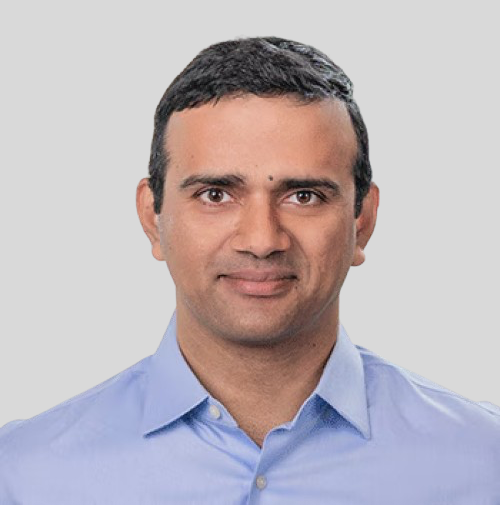
Moderator
Rajesh Ramanujam
Applied Ventures

Moderator
Laura Swan
Silicon Catalyst

Moderator
Reserved
TDK Ventures


Moderator
Yvonne Lutsch, Ph.D.
Lam Capital
Yvonne joined Lam Capital in October 2024 as Investment Director, bringing over 7 years of venture capital experience from Bosch Ventures USA, where she led investments in deep tech fields like AI, quantum computing, semiconductors, sensors, and industrial technology. She also has 13+ years of operational experience at Bosch, having served in leadership roles across technology scouting, business development, engineering, and manufacturing in both mobility as well as consumer electronics. Yvonne holds a PhD in Applied Physics from University of Tuebingen and a Diploma in Experimental Physics from University of Siegen, both Germany.
Lam Capital invests in innovative companies that are addressing some of today’s most challenging, high-impact problems. From semiconductor subsystems to AI chips and Industry 4.0 technologies, we invest in and partner with startups that are disrupting their respective industries.

Moderator
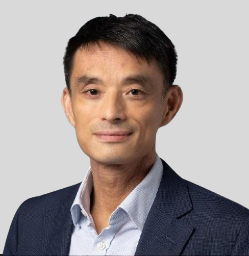
Walter Liu
Applied Ventures
Walter Liu is a Principal at Applied Ventures. As a passionate investor and value creator for his entire career, Walter has led both strategic and financial venture investments for multi-international technology corporations since 2016. His venture capital investments have spanned across AI, semiconductors, cloud, mobile, automotive, IoT and enterprise software. Before joining Applied Ventures, Walter was the Head of US investment at MediaTek Capital. Prior to transitioning into venture capital, Walter was a senior strategic marketing manager at Qualcomm and a wireless product manager at Huawei and Nokia. He also has seven years of ASIC application and system engineering experience at Qualcomm, Motorola and LCC International, where he designed AT&T’s 3G network in Los Angeles and supported base station OEMs to deploy 3G networks around the world. Walter has an MBA in finance and entrepreneurship from Cornell University and an M.S. in electrical engineering from UCLA.
Applied Ventures, LLC, is the venture capital arm of Applied Materials, Inc., (NASDAQ: AMAT). Applied Materials is the global leader in materials engineering solutions used to produce virtually every new chip and advanced display in the world. For more than a decade, Applied Ventures has invested in startups that are pioneering innovations in smartphones, augmented and virtual reality, AI, driverless cars, big data, life sciences, 3D printing, robotics, cleantech, and advanced materials. Applied Ventures is stage agnostic and invests up to $100M per year globally. We have invested in over 90 companies across 18 countries.

Moderator
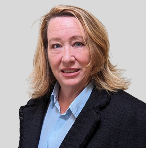
Laura Swan
Silicon Catalyst Ventures
Laura is in charge of portfolio company management at SCV. Laura is a Managing Partner with Silicon Catalyst and the Vice President of Operations for Silicon Catalyst Angels as well as an investor with Sand Hill Angels and a founding partner of The Batchery, a tech incubator in Berkeley California.
Laura earned her Master Degree in Electrical Engineering from the University of Wyoming (Go Pokes!).
Silicon Catalyst Ventures was formed as an extension of Silicon Catalyst, the world’s only incubator + accelerator focused on semiconductor solutions, including Photonics, MEMS, sensors, IP, materials and Life Science. It was formed primarily, but not exclusively, to fund and foster Silicon Catalyst Portfolio Companies. This close association between the Venture Fund and the Silicon Catalyst incubator affords investors unique access to entrepreneurial teams whose technology and businesses are accelerated and de-risked throughout a rigorous screening process and two year incubation.


Panelist
Mahyar Khosravi, P.Eng
Nitride Global
As Chairman and CEO, Mahyar oversees strategy and execution, while facilitating relationships and partnerships for Nitride Global. Over the past 20 years, he has worked with several companies of various sizes on technology strategy and engineering processes, utilizing emerging technologies to create automation and efficiencies. Through these roles, Mahyar has had the opportunity to work with sector leading companies such as Shell, Exxon Mobil, Rio Tinto, Saudi Aramco, Keppel, FANUC, Daimler, and BMW, amongst many others. In addition to his role at Nitride, Mahyar also currently serves as an advisor and board member to a number of companies, including Pocket Pills, The Pyure Company, Garmentier, and Dianomix.
Company Profile
Nitride Global Inc. is an early growth-stage company that has commercialized high volume processes to produce nitride substrates and nitride coatings. NSI’s substrates are enabling UVC light-emitting devices and detectors, as well as piezoelectric devices and high-speed communications chips. Its thin aluminum oxynitride coatings on copper and aluminum provide high-voltage insulation together with a 80x reduction in thermal resistance for electronic packaging.


Panelist
Farrokh Ayazi, Ph.D.
StethX Microsystems
Farrokh Ayazi is the Founder and CEO of StethX Microsystems, a spin-off of the Georgia Tech Integrated MEMS Laboratory that is commercializing advanced wearable patches for cardiopulmonary applications. He received the B.S. degree from the University of Tehran, Iran, in 1994, and the M.S. and Ph.D. degrees from the University of Michigan, Ann Arbor, in 1997 and 2000, respectively, all in electrical engineering. Dr. Ayazi is the Regents Entrepreneur and Ken Byers Professor in Microsystems at the Georgia Institute of Technology, where his main research interest lies in the area of integrated Micro/Nano-Electro-Mechanical-Systems (MEMS and NEMS), with a focus on high-Q acoustic resonators and advanced inertial sensors. Dr. Ayazi was the co-founder and CTO of Qualtré, a spin-out of his research laboratory that commercialized bulk acoustic wave silicon gyroscopes for high precision applications, which was acquired by Panasonic in 2016. Dr. Ayazi is a fellow of the IEEE, has authored over 300 refereed technical and scientific articles, and holds more than 60 patents. He was the general chair of the IEEE Micro-Electro-Mechanical-Systems conference in 2014, held in San Francisco, CA.
Company Profile
StethX is a start-up company located in Atlanta, GA commercializing a proprietary wearable sensor technology that enables remote and long-term monitoring of cardio-pulmonary conditions with high fidelity.


Panelist
Coralie Gallis Ph.D.
SM24
Coralie, a PhD in Materials Sciences from Paris University with an engineering degree in Physic- Chemistry, has over 25 years of experience in wearable sensing, medical and sports technology, semiconductors, and automotive industries. Previously in Silicon Valley and now in Las Vegas, Coralie has led business development and strategic partnerships in AI, biomedical tech, and wearable electronics. She is a co-founder and CTO of SM24, a wearable start-up, a non-invasive continuous biomarker monitoring system for metabolic health for the femtech, wellness and sport sector. Previous to the creation of the start-up, Coralie has been working in consumer technology industry within 2 different European semiconductors research centers dedicated to developing prototypes for industry partners. She has been a judge for the CES innovation awards the last 2 years. Since 2024, Coralie has also supported Vibra-Nova’s ultrasonic haptic technology expansion in the U.S.
Company Profile
SM24’s mission is to improve health and wellness while educating users in how to maintain good metabolic health and staying healthy.
Company Products & Services
SM24 is developing a wearable device, “patchable”, containing built-in multi sensors that monitor the level of glucose and, lactate within the sweat. These levels combined together with the activity will determine the metabolic usage of the person, whether that person consumes carb or fat to fuel.


Panelist
Cenfire Corporation
Seena Partokia is the founder and CEO of Cenfire, a next-generation MEMS switch company spun out of Atomica. Cenfire recently closed its Seed round and is now raising a Series A to scale commercialization of its solid-state switching platform, which combines ultra-low power consumption, high reliability, and fast switching speeds for demanding applications across automotive, defense, aerospace, and energy storage.
A lifelong obsession with transistors and switches has defined Seena’s path. He began his career working on RF switches using Silicon-on-Sapphire (SOS) and Silicon-on-Insulator (SOI) technologies, where he gained a deep understanding of device physics and analog performance. He then transitioned into the power semiconductor space, working on high-voltage devices and system-level reliability challenges. That journey led him to Menlo Micro, a MEMS relay company that raised over $230 million, where he contributed to product development and commercialization of MEMS switching technologies.
Throughout his career, Seena has worked exclusively on switches — from RF to power to MEMS — building deep expertise in device design, process integration, and go-to-market strategy. With Cenfire, he’s bringing those experiences together to develop a scalable, robust switching platform designed to replace incumbent relays across industries where size, weight, speed, and reliability matter most.
Company Profile
Cenfire is unlocking a new era of MEMS switching with an all-silicon platform that leverages the same scalable, proven infrastructure that has powered the semiconductor industry for decades. Built entirely on standard silicon, the technology delivers high-voltage handling, low-loss operation, and fast switching performance comparable to electromechanical relays—without relying on esoteric material sets, exotic fabrication processes, or unscalable design philosophies. Rather than attempting to fabricate complex structures from rare materials, Cenfire uses the most abundant, cost-effective, and industrially mature material on Earth to address the toughest switching challenges in power and signal electronics.
The company’s MEMS relay platform is based on a modular unit cell architecture that can be arrayed in series or parallel to support a wide range of voltage and current requirements. This architecture enables precise, application-specific optimization—combining the speed and longevity of solid-state switches with the galvanic isolation and power-handling capabilities of mechanical relays. Cenfire’s silicon-based MEMS switches are orders of magnitude smaller and faster than traditional relays, with dramatically reduced power consumption and footprint—ideal for compact, high-performance systems.
From aerospace and defense to electric vehicles, renewable energy systems, and high-efficiency power converters, Cenfire delivers chip-scale switching performance to markets long limited by the size, speed, and inefficiencies of legacy relay technologies. Like every transformative hardware platform before it, this is the future of switching—built on silicon, again.


Panelist
Aftab Farooqi, Ph.D.
ChipHub
Aftab is the founder and CEO of ChipHub, an AI enabled semiconductor SaaS procurement platform for the hardware industry. ChipHub is Aftab’s second start-up. He was the founder and CEO of SiliconXpress, an IC design firm in 2008. Aftab began his career as an IC designer in the late 1980’s and has held a variety of both technical and commercial leadership roles including the last 12 years in semiconductor sourcing at Google and Amazon. He has a PhD in Electrical Engineering (VLSI design) from Texas Tech University.
Company Profile


Panelist
Cris Ugolini, Ph.D.
Alithia Power
Since grad school, Cris has been developing and commercializing III-N materials and devices. From all levels of business, he is an experienced and proven expert in innovating products for both large and small enterprises. Starting with the LED revolution at CREE, UVC LEDS and substrates at Nitride Solutions, and GaN-based power electronics at Kyma, Cris is a proven expert in developing and innovating most applications that III-N materials have to offer. He has two undergraduate degrees in math and physics from Bethany college, and a Ph.D in materials science at Kansas State University.
Company Profile
Alithia Power inc. (API) is a seed-stage company in the Raleigh-Durham area of North Carolina. Founded in January of 2023, API aims to be a high-volume manufacturer of vertical GaN power electronics for segments of the electrification market like electric vehicles, industrial motors, data rooms, renewable energy, and the SMART grid. Our products are branded as vertiGANTM.


Panelist
Nilesh Gharia
Numem
Nilesh has 20+ years of experience in the semiconductor industry with a diverse background in semiconductor design and product development. Nilesh was part of the startup team at NetLogic Microsystems which went IPO in 2004, and was later acquired by Broadcom in 2012 for $3.7B, which in turn was acquired by Avago in 2016 for $37B. He was also the 1st Engineer at Lanstar Semiconductor, which also went IPO. Nilesh worked in Virtual Silicon Technology, and was responsible for team development and product design. His expertise includes startups, emerging memories, memory compiler development, MRAM technologies, semiconductor IP development, network processors, and team/project management. Nilesh holds a Masters in Electrical Engineering from the New Jersey Institute of Technology and has a portfolio of 13 US issued patents.
Numem, headquartered in Sunnyvale, California, is the leading provider of advanced SOC Compute in Memory based on its patented NuRAM (MRAM) and SOC Subsystem IP Cores and Chiplets based on its patented, RISC-based, SmartMem technologies. Numem NuRAM provides an excellent SRAM and eFlash alternative for SoC Designers/ Architects with 2.5x smaller area and >20x lower leakage power than SRAM.
Numem provides an end-to-end solution that is disrupting the semiconductor industry by enabling ultra-low power, high-performance integration of persistent memory that can be down without losing data.
Numem’s IP Cores and Chiplets are used in IoT/Wearables, AI/Generative AI, Digital Security/Cameras, Autonomous Vehicle and Data Center applications. They enable Customers with a substantial reduction in system power and time to market.
Visit our website http://www.numem.com or contact us at sales@numem.com.

18:30 – 20:30
Closing Cocktail Reception at Plug & Play TC Terrace
End of content
End of content