


未来を牽引する:半導体産業における先進的なパッケージング、AIの統合、そして自動車のイノベーション
08:00 – 08:35
受付(登録)
次世代半導体およびパッケージングソリューションにおけるガラスおよび パネル基板の進化した基板技術
08:40 – 09:00
基調講演
Advanced Packaging Technologies for the AI era
Advanced packaging is enabling unprecedented levels of integration, enabling dense interconnection of logic, memory and optical chiplets, to create a system in a package. In AI & data centric applications, the amount of silicon content in a single package is increasing dramatically every generation. To meet future scaling, high speed signaling and power delivery needs, the package substrate must also evolve significantly. In this talk, we will cover some of the recent advances in the EMIB package platform including multiple scaling vectors such as die to die interconnection pitch, package form factor and the introduction of a bridge with TSV to enable denser and more efficient integration on package. Further, we will also cover the Intel’s latest breakthrough’s in glass core substrates which have superior mechanical, physical and optical properties and can drive dramatic improvements in chiplet integration on a substrate.
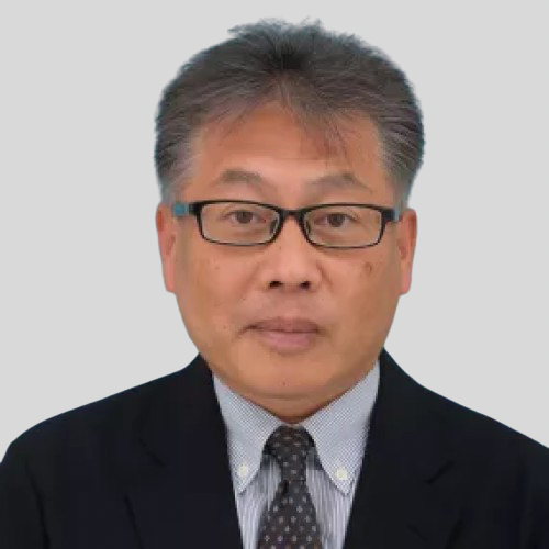
ラーフル・マネパリ博士
Intel Fellow & Vice President : Advanced Packaging Technology Development
Intel - Rahul Manepalli Ph.D., Intel Fellow, VP, Director of Substrate Packaging Technology Development
Dr. Rahul Manepalli is an Intel Fellow, Vice President and Director of the Substrate & Wafer Assembly Technology Development organization in Intel. He currently leads the IC substrate technology development and 3DIC wafer assembly technology development teams in Intel’s Advanced Packaging Technology and Manufacturing Organization. He and his team are driving the pathfinding & development of materials, processes and equipment for the next generation of substrate, wafer level assembly technologies. His team has been the driving force behind many of the technology innovations in Intel’s Embedded Multi-die Interconnect Bridge (EMIB/EMIB-T), Panel ODI, Glass core substrate, Foveros (Solder and HBI die to wafer interconnect) technologies. Over his 25+ year career at Intel, Rahul has also held leadership roles in Intel’s assembly materials development and pathfinding teams leading to several innovations in encapsulants, thermal interface materials and solder alloys. Rahul is the author of over 250 patent publications in semiconductor packaging, over 50 technical papers and invited talks. He has a Ph.D. in Chemical Engineering from the Georgia Institute of Technology.
会社概要
Intel (Nasdaq: INTC) is an industry leader, creating world-changing technology that enables global progress and enriches lives. Inspired by Moore’s Law, we continuously work to advance the design and manufacturing of semiconductors to help address our customers’ greatest challenges. By embedding intelligence in the cloud, network, edge and every kind of computing device, we unleash the potential of data to transform business and society for the better.
To learn more about Intel’s innovations, go to newsroom.intel.com and intel.com.

09:00 – 09:20
基調講演
Brightening the Future with Advanced Semiconductor Packaging Technologies
At the forefront of semiconductor technology development, the evolution of back-end processes is essential. In particular, “advanced semiconductor packaging technology” is responding to the demand for high performance and multi-functionality of semiconductors and promoting high integration. In this presentation, we will introduce the latest technological trends.
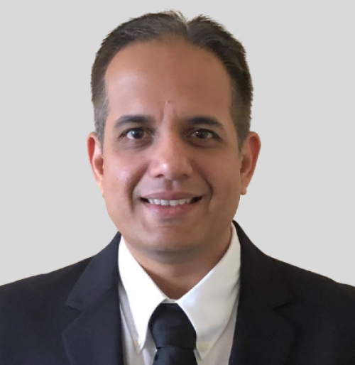
荒木 康 氏
Corporate Officer
新光電気工業株式会社
Graduated from Applied Chemistry, Nagoya University in 1989.
1989-2000: Joined Fujitsu Ltd. Engaged in IC assembly technology.
2000-2021: Joined Shinko Electric Industries Co., Ltd. Engaged in IC Assembly technology.
From 2021: Engaged in Research and Development in the R&D Div.
会社概要
SHINKO is a worldwide semiconductor packaging supplier with diverse technology driven initiatives and industry leading manufacturing capabilities.
09:20 – 09:40
Revisiting the Necessity and Challenges of Glass Substrates in 3DIC Advanced Packaging
In 3DIC and HPC packaging, achieving both high-precision assembly and reliability demands a careful balance of material properties. Glass offers low CTE, high flatness, and low dielectric loss, yet faces trade-offs such as TGV reliability and stress management. This study argues that, without clearly defining the necessity of glass, application development lacks momentum. By analyzing these inherent contradictions, we discuss how to interpret and manage the trade-offs between material properties and system reliability, providing insights toward the future direction of glass utilization in advanced packaging.
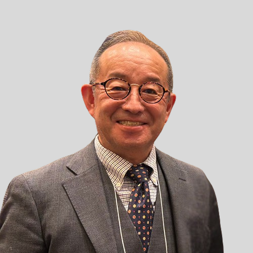
市川 公也 氏
テクニカル ディレクター
3DIC Research Lab
Kinya Ichikawa retired from TSMC Japan 3DIC R&D Center Inc. as Technical Director in September 2024 and subsequently founded 3DIC Research Lab LLC, providing technical consulting for Japan’s semiconductor packaging ecosystem. At TSMC, he led the establishment of the Tsukuba R&D Center, aligned R&D with Taiwan headquarters, and managed NEDO project planning and execution. Before joining TSMC, he directed a joint development project at Nichia Corporation with European partners on next-generation high-definition micro-LED headlamps, which entered mass production in 2024. Earlier, he spent 24 years at Intel, pioneering FCBGA (OLGA) and EMIB technologies.
会社概要
3DIC Research Lab LLC is a specialized consulting firm dedicated to advancing semiconductor packaging technologies with a focus on 3D integration. Founded by experts with decades of experience in wafer-level packaging, TSV, hybrid bonding, and advanced substrate technologies, the company provides deep technical insights and strategic guidance to semiconductor manufacturers, material suppliers, and equipment vendors. 3DIC Research Lab operates as a bridge between cutting-edge academic research and industrial applications, helping partners accelerate innovation, reduce risks, and optimize manufacturing processes. With strong expertise in areas such as HBM integration, fan-out packaging, and chiplet-based architectures, the company supports its clients in addressing key challenges in power, performance, thermal management, and reliability. By combining technical consulting with market perspectives, 3DIC Research Lab contributes to the realization of next-generation semiconductor solutions for AI, HPC, and consumer electronics.
Company Products & Services
3DIC Research Lab LLC offers a comprehensive range of consulting services tailored to the semiconductor packaging ecosystem. Its core services include technology evaluation, material selection support, process integration strategies, and roadmap development for advanced packaging solutions. The company provides in-depth technical analysis on critical areas such as wafer thinning, TSV formation, RDL scaling, underfill materials, and thermal interface solutions. Additionally, 3DIC Research Lab delivers customized training programs, workshops, and technical seminars to support knowledge transfer and skill development within client organizations. By leveraging a strong global network and hands-on expertise, the firm helps clients benchmark emerging technologies, assess competitive landscapes, and establish collaborations across the supply chain. Whether guiding material suppliers to meet stringent reliability requirements or advising device makers on cost-performance trade-offs, 3DIC Research Lab ensures that its partners are equipped to navigate the complexities of heterogeneous integration and advanced packaging.
09:45 – 10:45
ネットワーキング・ビジネスミーティング5・6
10:50 – 11:00
Tailoring through glass via (TGV) dimensions for glass-core panel substrates
Glass-core substrates are redefining advanced packaging by overcoming warpage and thermal management limits of organic materials. Central to this technology are through-glass vias (TGVs), whose precision and density define performance. We present an innovative alkaline etching technology combined with laser modification, enabling unprecedented control of via geometry with taper angles below 1°. Compared to conventional acidic etching, our process delivers higher selectivity, at advanced throughput, and compatibility with industrial considered glass types. This breakthrough enables the scalable production of ultra-high-density TGV substrates—paving the way for next-generation packaging demands.
Holger H. Kuehnlein氏, PhD,
SVP Technology
RENA Technologies
Holger H. Kuehnlein began his career in 1999 at the Technical University of Dresden, within Silicon Saxony, gaining early industrial experience in ECD for packaging. His PhD work on Cu2ZnSn for CZTS semiconductors at ATOTECH led him to RENA Technologies in 2007, where he propelled PV success in PERC, TOPCON, and IBC cell technologies. Since 2015, as Head of Technology & Innovation at RENA, he has significantly contributed to the SEMI industry, diversifying into mobile device glass components, semiconductor wafering, plating, and Lithium-ion batteries. Currently, he focuses on wet chemical Through-Glass Via (TGV) etching and metallization of Glass Core Panel Substrates for advanced packaging in HPC/AI, collaborating with key industry players. His team also innovates electrochemical methods for SiC, Si (epitaxial-wafering), GaN, and GaO in next-gen power applications.
会社概要
Founded in 1993, RENA Technologies has established itself as a global leader in mechanical and process engineering, for a diverse range of industries. We specialize in providing cutting-edge wet processing solutions for the semiconductor, solar, additive manufacturing, glass, and medtech industries.
A key area of expertise is wet chemical immersion, spray and single wafer processes for the manufacturing of semiconductors. With over 1,100 systems installed worldwide, our technology is trusted by manufacturers around the globe to enhance efficiency and production quality.
RENA Technologies employs approximately 1,000 professionals worldwide, all dedicated to innovation and excellence in our field. Headquartered in Gütenbach, Germany, and manufacturing sites in Albany, OR and Wykroty, Poland, we continue to drive advancements in process engineering, ensuring our customers receive the highest quality solutions for their manufacturing needs.
On top we provide worldwide onsite service support with over 150 Experts in 20 locations globally to ensure flawless installation and operation of our tools.
Company Products & Services
RENA products are used in path-breaking application fields such as semiconductors, MedTech, renewable energies, the glass industry and additive manufacturing. RENA equipment is used to treat or modify surfaces of, for example, semiconductor wafers, solar cells, glass, optical substrates, 3D-printed metal components or other high-tech products using wet chemical processes like etching, stripping, cleaning or drying. RENA offers proven standard machines as well as customer-specific solutions and process support.
11:00 – 11:10
包装技術の進化:シリコンインターポーザー代替としてのガラスコア統合に向けたガラスビアの探求
In contemporary electronic packaging, the pursuit of miniaturization, enhanced performance, and reliability remains a fundamental driving force. This abstract introduces a novel approach in advanced packaging through the utilization of Through Glass Vias (TGVs) for Glass Core Integration, as a viable alternative to Conventional Silicon (Si) Interposer technology. The presentation encapsulates the background, motivations, technical aspects, and results of our evaluation work in this innovative packaging paradigm.
The background of this research is grounded in the growing demand for smaller form factors, increased functionality, and improved thermal management in electronic devices. Traditional Si interposer technology, while effective, presents limitations in terms of scalability, thermal conductivity, and electrical performance. Thus, the exploration of alternative materials and methodologies is imperative for the next generation of packaging solutions.
Motivated by the exceptional properties of glass, including its thermal stability, electrical insulation, and compatibility with existing manufacturing processes, this study delves into the feasibility of utilizing glass as both a carrier and core material in advanced packaging. Through Glass Vias (TGVs) emerge as a key enabler, facilitating vertical interconnects within the glass substrate.
Key considerations such as through-hole requirements, aspect ratios, seed layer deposition, and adhesion to glass are meticulously addressed to ensure the integrity and reliability of the packaging structure. Innovative process technologies are developed to fabricate TGVs with precise dimensions, high aspect ratios, and robust electrical properties.
The hardware requirements for implementing TGV-based packaging are evaluated, encompassing equipment for laser drilling, seed layer deposition, plating, and planarization processes. Cost considerations are also examined to ascertain the economic viability of this approach compared to conventional methodologies.
Results from our evaluation work demonstrate promising advancements in TGV-based packaging, including enhanced electrical performance, superior thermal dissipation, and significant miniaturization potential. Through detailed analysis and experimentation, this presentation illuminates the transformative capabilities of Through Glass Vias for Glass Core Integration, heralding a new era in advanced packaging technology.
Herbert Oetzlinger
VP and Head of Panel Product Line
Lam Research ラムリサーチ合同会社
Herbert Oetzlinger , graduated HTL Braunau 1987 in high power electronics/ electrotechnics.
Herbert worked in the Semiconductor industry for 30+ years, focused on wet processing .
Special focus on advanced packaging in electroplating and wet etching/cleaning of wafers and substrates. For many years he was VP of Sales with Semitool Inc, where he excelled with his in-depth knowledge of process and hardware. During this time, Herbert worked with many worldwide leading companies on Fan-out, E-WLB and other new developments in wafer level advanced packaging.
In 2012, he founded Semsysco GmbH and is also heading the company as CEO.
LAM – Semsysco is a world leader in high speed electrochemical deposition with a pedigree and expertise in all-around wet processing for wafer and panel level.
会社概要
Lam Research Corporation is a trusted global supplier of innovative wafer fabrication equipment and services to the semiconductor industry. Our strong values-based culture fuels our progress, and it’s through collaboration, precision, and delivery that we are driving semiconductor breakthroughs that define the next generation. Lam Research (Nasdaq: LRCX) is a FORTUNE 500® company headquartered in Fremont, California, with operations around the globe. Learn more at www.lamresearch.com
Company Products & Services
We combine superior systems engineering, technology leadership, and a commitment to customer success to advance the global semiconductor industry. Our broad portfolio of market-leading deposition, etch, strip, and wafer cleaning solutions helps customers achieve success on the wafer by enabling device features that are 1,000 times smaller than a grain of sand—it’s why nearly every chip today is built with Lam technology.
11:10 – 11:20
Orbital Manufacturing of Next-Generation Semiconductors
The growing commercial space economy is lowering launch costs and enabling the construction of large-scale orbital infrastructure, paving the way for industrialization in space. The unique conditions of LEO – such as the absence of convection and the availability of high vacuum – can enable the growth of large defect-free crystals of WBG semiconductors, photonics, and quantum materials which cannot be produced at commercial scale on the ground today. This will unlock new levels of performance and efficiency in critical applications like electric vehicles, renewable energy, and advanced computing.
This talk will explore how commercial space stations, space logistics providers and large-scale orbital infrastructure are together unlocking the production of next-generation semiconductors in space. It will also highlight commercial case studies demonstrating the feasibility and potential of this transformative technology.
Koichi Wakata
Astronaut and Chief Technology Officer
Axiom Space
Koichi Wakata is a veteran astronaut and globally recognized space leader who spearheads Axiom Space’s strategic expansion in the Asia-Pacific region and provides critical insight for the development of Axiom Station, the world’s first commercial space station. Wakata holds the Japanese record for the most space flights (five) and longest cumulative time in space (504 days). He made history as the first Japanese Shuttle Mission Specialist (1996) and the first Japanese ISS Commander (2014). He brings over 33 years of human spaceflight experience, having previously served as JAXA Vice President and ISS Operations Branch Chief of the NASA Astronaut Office.
会社概要
Axiom Space is the leading developer of next-generation orbital infrastructure and provider of human spaceflight services. Axiom Space is building the world’s first commercial space station, Axiom Station, and orbital infrastructure for orbital data centers and in-space manufacturing of semiconductors and pharmaceuticals. The company is pushing the boundaries of technological innovation and providing end-to-end solutions for the semiconductor industry to expand its research and manufacturing capabilities beyond Earth. Axiom Station and its scalable orbital infrastructure will enable the manufacturing of next-generation semiconductor materials for energy, compute, quantum, and automotive applications on the ground. Axiom Space is furthering American leadership in space exploration, elevating national space programs globally, and enabling the industrialization of space by redefining the pathway to sustained presence in the low-Earth orbit.

11:25 – 12:10
Panel Discussion: How Far Can Package and Substrate Scaling Go Beyond 2028?
モデレーター
市川 公也 氏
テクニカル ディレクター
3DIC Research Lab
Kinya Ichikawa retired from TSMC Japan 3DIC R&D Center Inc. as Technical Director in September 2024 and subsequently founded 3DIC Research Lab LLC, providing technical consulting for Japan’s semiconductor packaging ecosystem. At TSMC, he led the establishment of the Tsukuba R&D Center, aligned R&D with Taiwan headquarters, and managed NEDO project planning and execution. Before joining TSMC, he directed a joint development project at Nichia Corporation with European partners on next-generation high-definition micro-LED headlamps, which entered mass production in 2024. Earlier, he spent 24 years at Intel, pioneering FCBGA (OLGA) and EMIB technologies.
会社概要
3DIC Research Lab LLC is a specialized consulting firm dedicated to advancing semiconductor packaging technologies with a focus on 3D integration. Founded by experts with decades of experience in wafer-level packaging, TSV, hybrid bonding, and advanced substrate technologies, the company provides deep technical insights and strategic guidance to semiconductor manufacturers, material suppliers, and equipment vendors. 3DIC Research Lab operates as a bridge between cutting-edge academic research and industrial applications, helping partners accelerate innovation, reduce risks, and optimize manufacturing processes. With strong expertise in areas such as HBM integration, fan-out packaging, and chiplet-based architectures, the company supports its clients in addressing key challenges in power, performance, thermal management, and reliability. By combining technical consulting with market perspectives, 3DIC Research Lab contributes to the realization of next-generation semiconductor solutions for AI, HPC, and consumer electronics.
Company Products & Services
3DIC Research Lab LLC offers a comprehensive range of consulting services tailored to the semiconductor packaging ecosystem. Its core services include technology evaluation, material selection support, process integration strategies, and roadmap development for advanced packaging solutions. The company provides in-depth technical analysis on critical areas such as wafer thinning, TSV formation, RDL scaling, underfill materials, and thermal interface solutions. Additionally, 3DIC Research Lab delivers customized training programs, workshops, and technical seminars to support knowledge transfer and skill development within client organizations. By leveraging a strong global network and hands-on expertise, the firm helps clients benchmark emerging technologies, assess competitive landscapes, and establish collaborations across the supply chain. Whether guiding material suppliers to meet stringent reliability requirements or advising device makers on cost-performance trade-offs, 3DIC Research Lab ensures that its partners are equipped to navigate the complexities of heterogeneous integration and advanced packaging.

Panelist
Deepak Kulkarni, Ph.D.
シニア・フェロー アドバンスド・パッケージング
AMD
Deepak Kulkarni is a Senior Fellow at Advanced Micro Devices (AMD), where he leads the Instinct and Optics Technology Development team. In this role, he develops heterogeneous architectures for AMD’s AI accelerator products and oversees Photonics technology development.
With twenty years in technology development, Deepak has led the development of several innovative technologies such as panel-level fan-out, Embedded Multi-die Interconnect Bridge (EMIB), Elevated Fan-Out Bridge (EFB), and 3.5D packaging solutions. Recognized with top awards at both AMD and Intel, and a frequent voice on high-level industry panels, Deepak brings both technical depth and strategic vision to advancing heterogeneous integration.
Deepak’s technical interests cover Co-packaged Optics, Panel-level packaging, and design-technology co-optimization. He holds forty patents and has published over twenty papers. He earned his PhD in Mechanical Engineering with a minor in Computational Science from the University of Illinois at Urbana-Champaign.
会社概要
For 50 years, AMD has driven in high-performance computing, graphics, and visualization technologies – the building blocks for gaming, immersive platforms, and the datacenter. Hundreds of millions of consumers, leading Fortune 500 businesses and cutting-edge scientific research facilities around the world rely on AMD technology daily to improve how they live, work and play. AMD employees around the world are focused on building great products that push the boundaries of what is possible. For more information about how AMD is enabling today and inspiring tomorrow, visit AMD (NASDAQ:AMD) on their website, blog, Facebook and Twitter pages.

Panelist
ラーフル・マネパリ博士
Intel Fellow & Vice President : Advanced Packaging Technology Development
Intel - Rahul Manepalli Ph.D., Intel Fellow, VP, Director of Substrate Packaging Technology Development
Dr. Rahul Manepalli is an Intel Fellow, Vice President and Director of the Substrate & Wafer Assembly Technology Development organization in Intel. He currently leads the IC substrate technology development and 3DIC wafer assembly technology development teams in Intel’s Advanced Packaging Technology and Manufacturing Organization. He and his team are driving the pathfinding & development of materials, processes and equipment for the next generation of substrate, wafer level assembly technologies. His team has been the driving force behind many of the technology innovations in Intel’s Embedded Multi-die Interconnect Bridge (EMIB/EMIB-T), Panel ODI, Glass core substrate, Foveros (Solder and HBI die to wafer interconnect) technologies. Over his 25+ year career at Intel, Rahul has also held leadership roles in Intel’s assembly materials development and pathfinding teams leading to several innovations in encapsulants, thermal interface materials and solder alloys. Rahul is the author of over 250 patent publications in semiconductor packaging, over 50 technical papers and invited talks. He has a Ph.D. in Chemical Engineering from the Georgia Institute of Technology.
会社概要
Intel (Nasdaq: INTC) is an industry leader, creating world-changing technology that enables global progress and enriches lives. Inspired by Moore’s Law, we continuously work to advance the design and manufacturing of semiconductors to help address our customers’ greatest challenges. By embedding intelligence in the cloud, network, edge and every kind of computing device, we unleash the potential of data to transform business and society for the better.
To learn more about Intel’s innovations, go to newsroom.intel.com and intel.com.

Panelist
Cleon Chan
VP, Business Development (Panel Solutions)
Onto Innovation
Cleon Chan is the Vice President, Business Development for the Panel Solutions for Onto Innovation since 2019 after merger between Rudolph Technologies and Nanometrics. He worked with many companies on FOPLP, Interposer and Substrate (2.xD, 2.5D and 3D Heterogeneous Integration) to identify challenges and how Onto Steppers, Inspection/Metrology and Yield solutions can enable the Advanced IC Substrate and Packaging roadmap. Previously, he was with Rudolph Technologies as Global Sales and Applications in 2015. Prior to Rudolph, he was with Applied Materials as Strategic Marketing GM and was responsible for some key process equipment for both Advanced Packaging and Frontend processes. He also held management positions at Varian Semiconductor and STEAG Microtech before joining Applied Materials. Cleon graduated with Bachelor of Electrical and Electronics Engineering (Hons) from National University of Singapore.
会社概要
Onto Innovation is a leader in process control, combining global scale with an expanded portfolio of leading-edge technologies that include: Un-patterned wafer quality; 3D metrology spanning chip features from nanometer scale transistors to large die interconnects; macro defect inspection of wafers and packages; elemental layer composition; overlay metrology; factory analytics; and lithography for advanced semiconductor packaging. Our breadth of offerings across the entire semiconductor value chain helps our customers solve their most difficult yield, device performance, quality, and reliability issues. Onto Innovation strives to optimize customers’ critical path of progress by making them smarter, faster and more efficient. Headquartered in Wilmington, Massachusetts, Onto Innovation supports customers with a worldwide sales and service organization.
General Telephone: +1 978 253 6200
General email: info@ontoinnovation.com
Website: www.ontoinnovation.com


Panelist
阿部 秀則 氏
執行役員 半導体材料研究開発統括
株式会社レゾナック
Hidenori Abe is CTO for semiconductor materials and Executive Director of Electronics Business Headquarters at Resonac. He leads R&D and strategy for electronic materials in semiconductors, substrates, and displays. Previously, Mr. Abe served as the head of the Electronics R&D Center and Packaging Solution Center, where he contributed to advanced packaging development through open innovation. Notably, in 2021, he directed the launch of JOINT2, a consortium targeting 2.xD and 3D packaging technologies. He received a master’s degree in chemical engineering from Tokyo Institute of Technology, Japan, and a master’s degree in the Executive MBA program from the University of Oxford, UK.
会社概要
Resonac defines its purpose as “Change society through the power of chemistry.” Resonac aims to be a world-class functional chemical manufacturer, creating functions necessary for the times, supporting technological innovation, and contributing to the sustainable development of our customers. Resonac is Global Leading semiconductor materials supplier. In order to achieve technological innovation for solving various social issues, it is essential for us to make wide-ranging co-creative efforts with partners, and Resonac is open to collaboration including 1on1 co-development with any partner.
We have opened a Packaging Solution Center and are actively engaged in next-generation semiconductor co-creation activities through JOINT2 with many partner companies. Furthermore, starting this year, we will also seek co-creation opportunities in the United States by launching US-JOINT.

Panelist
荒木 康 氏
Corporate Officer
新光電気工業株式会社
Graduated from Applied Chemistry, Nagoya University in 1989.
1989-2000: Joined Fujitsu Ltd. Engaged in IC assembly technology.
2000-2021: Joined Shinko Electric Industries Co., Ltd. Engaged in IC Assembly technology.
From 2021: Engaged in Research and Development in the R&D Div.
会社概要
SHINKO is a worldwide semiconductor packaging supplier with diverse technology driven initiatives and industry leading manufacturing capabilities.
12:15 – 13:30
昼食
最先端のイノベーションでパワー半導体と自動車の未来を形作る
13:35 – 13:55
基調講演
次世代車両が直面する電力課題と村田製作所の技術革新への取り組み
Vehicle architecture is undergoing rapid transformation driven by autonomous driving, IoT integration, AI implementation, and the shift toward Software-Defined Vehicles (SDVs). The overall power consumption of vehicles is increasing due to the rise in electronic control units and the adoption of high-performance processors. While low-power design, wide bandgap semiconductors, and thermal management technologies are being developed, efforts are also underway to develop in-motion charging and transition to 48V architectures.
Requirements for electronic devices in new architectures and Murata’s initiatives will be reported.
岩坪 浩 氏
代表取締役副社長
Murata Manufacturing
1985.Mar Hiroshi Iwatsubo graduated from Kyoto University, Department of Technology. He joined Murata Manufacturing Co., Ltd. in Kyoto, Japan in 1985. After engaging in the development of ceramic materials for four years, he was transferred to Murata Europe GmbH in 1989 until his return to Murata Japan in 1993.
In 2012, he was appointed to Vice President, Head of Global Sales & Marketing
In 2015, he was appointed to Senior Executive Vice President (Board Member) Corporate Technology & Business Development Unit, In 2020, Senior Executive Vice President .
Since 2024, Hiroshi Iwatsubo currently serves as CTO and Executive Deputy President.
会社概要
Murata Manufacturing Co., Ltd. is a worldwide leader in the design, manufacture and sale of ceramic-based passive electronic components & solutions, communication modules and power supply modules. Murata is committed to the development of advanced electronic materials and leading edge, multi-functional, high-density modules. The company has employees and manufacturing facilities throughout the world. For more information, visit Murata’s website at www.murata.com.
www.murata.com/en-global
Company Products & Services
Research, Production and Sales of Electronic Devices made from fine ceramics
13:55 – 14:15
半導体製造工場におけるAMHSの現在と未来を探る
Automated transportation in semiconductor fabs began with front-end processes in 1980s. It has grown in scale and expanded to advanced back-end operations. Recently we are also receiving requests to handle materials and tools. Beyond wafer transportation, by “Full Fab Automation”, where we fully automate the movement of goods throughout the entire factory, we aim to contribute to the ever-growing semiconductor industry.
村田大介 氏
代表取締役社長
村田機械株式会社
Daisuke Murata has served as President and CEO of Murata Machinery, since September 2003. He has held a variety of ascending leadership positions at Murata Machinery since 1987.
He also now serves as Chairman of the Japan Textile Machinery Association, as Chairman of the Japan Institute of Material Handling, and Superintendent of the Japan Business Machine and Information System Industries Association. In July 2017, he became the SEMI International Board member.
He graduated with a Bachelor of Economics from Hitotsubashi University in 1984 and obtained MBA from the Graduate School of Business at Stanford University in 1990.
会社概要
Murata Machinery (Muratec) is a worldwide leader and solution provider for automated material handling systems in semiconductor manufacturing and other manufacturing or distribution industries. Muratec also manufactures machinery and equipment such as Textile Machinery, Machine Tools, Sheet Metal Machinery, and Communication Equipment.
This year marks 90 years since its founding in 1935. Under the slogan “Innovation. Mark the turning point”, Muratec aims to create technologies that bring innovation to the market and society.
Company Products & Services
・Logistics & Automation Division
Logistics Center, Automated Storage & Retrieval Systems (AS/RS), Transportation Systems, Picking Systems, Sorting Systems, Data Management system
・Clean FA Division
Transport Systems & Storage Systems For Semiconductor fab.
・Machine Tools Division
CNC Twin-spindle Chucker, CNC Twin-spindle Turning Center, CNC Opposed Twin-spindle, FMC and FMS
CNC Turret Punch Press, CNC laser punch press,
Press Brake, Automatic CAD/CAM system for sheet metal working, FMC and FMS
・Textile Machinery Division
VORTEX Spinning Machines, Automatic Winders
・Communication Equipment Division
Digital Multifunctional Product, Laser Xerographic Printer Facsimile, LED Linear Array Optical Facsimile, Thermal Transfer Facsimile,
Document & IP Solutions

14:15 – 14:35
モビリティと持続可能性の推進:次世代パワーデバイスと統合パワー エレクトロニクスに向けたデンソーのビジョン
Achieving zero accidents and zero emissions demands breakthrough innovation in automotive power electronics. DENSO, drawing on its Tier1 expertise and the advanced semiconductor R&D of MIRISE Technologies, is driving progress in wide bandgap semiconductors, advanced packaging solutions, and next-generation control technologies through integrated system development. This approach enables higher efficiency and reliability in electrified vehicles and accelerates the transition to sustainable mobility. Through global collaboration and next-generation solutions, DENSO is committed to shaping a future where mobility harmonizes with environmental stewardship and societal wellbeing.
松ケ谷 和沖 氏
情報開発センター シニアディレクター
株式会社デンソー-
Dr. Kazuoki Matsugatani joined DENSO CORPORATION in 1989, and has over 25 years of R&D experience in electronics, including compound semiconductors, microwave and millimeter-wave circuits, wireless communication systems, and ADAS. He has held key leadership roles such as Director of R&D Division 3, Director of ADAS Business and Technology Development. In 2017, he became Executive Director and Head of Engineering in Europe, and in 2019, Executive Officer and Head of Engineering in North America. After returning to Japan, he was appointed Senior Director at DENSO CORPORATION in 2021, and joined MIRISE Technologies as a Member of the Board in 2022.
会社概要
DENSO is a €44.1 billion ($47.9 billion) global mobility supplier that develops advanced technology and components for nearly every vehicle make and model on the road today. With manufacturing at its core, DENSO invests in its around 200 facilities to produce electrification, powertrain, thermal, mobility electronics, advanced devices to create jobs that directly change how the world moves. The company’s around 158,000 employees are paving the way to a mobility future that improves lives, eliminates traffic accidents, and preserves the environment. Globally headquartered in Kariya, Japan, DENSO spent nearly 10 percent of its global consolidated sales on research and development in the fiscal year ending March 31, 2025.
In Europe, DENSO regional headquarters is located in Amsterdam, the Netherlands. DENSO has 36 official group companies located in 15 European countries and employs more than 13,000 people across its European organization. DENSO Europe’s consolidated revenue was €3.9 billion ($4.3 billion) for the fiscal year ending March 31, 2025.
14:35 – 14:45
スマート材料、より賢いシステム:設計基板による3D集積の実現
The semiconductor industry is entering a decisive phase where traditional 2D scaling is no longer sufficient to sustain performance, energy efficiency, and cost targets. The path forward lies in 3D integration, where materials innovation and substrate engineering play a pivotal role. At Soitec, our mission is to provide the foundational technologies that make this transition possible.
Engineered substrates represent a strategic enabler for the next era of computing. By tailoring the substrate to the device, we unlock unique advantages: superior electrical isolation, reduced power consumption, enhanced thermal performance, and the ability to integrate diverse materials seamlessly. This flexibility is essential to meet the diverse requirements of high-performance computing, mobile communications, automotive intelligence, and edge AI.
At the heart of this innovation is Soitec’s Smart Cut™ layer transfer technology. This breakthrough makes it possible to detach and transfer ultra-thin crystalline layers with atomic precision, enabling stacking and heterogeneous integration at a scale and quality unmatched in the industry. With Smart Cut™, we can bring logic, memory, and interconnect layers closer together, shortening critical paths, reducing latency, and dramatically increasing bandwidth density.
What this means for the industry is profound: engineered substrates and precision layer transfer redefine the scaling roadmap. They extend Moore’s Law where transistor scaling alone cannot, and accelerate “More-than-Moore” solutions by enabling chiplet architectures, advanced system-in-package, and vertically integrated designs.
As we look ahead, Soitec is committed to driving collaboration across the ecosystem—foundries, device makers, and system integrators—to unlock the full potential of 3D integration. By aligning materials innovation with system-level needs, we ensure that the semiconductor industry continues to deliver the performance and efficiency breakthroughs that power our digital society.
Christophe Maleville氏, Ph.D,
Chief Technology Officer and Senior Executive Vice President of Soitec’s Innovation
Soitec
Christophe Maleville has been appointed Chief Technology Officer and Senior Executive Vice President of Soitec’s Innovation.
He joined Soitec in 1993 and was a driving force behind the company’s joint research activities with CEA-Leti. For several years, he led new SOI process development, oversaw SOI technology transfer from R&D to production, and managed customer certifications. He also served as vice president, SOI Products Platform at Soitec, working closely with key customers worldwide.
Maleville has authored or co-authored more than 30 papers and also holds some 30 patents. He has a PhD in microelectronics from Grenoble Institute of Technology and obtained an executive MBA from INSEAD.
会社概要
Soitec is a world leader in the production of innovative semiconductor materials. The company leverages its unique technologies to serve the electronics markets.
In meeting the technical and economic challenges of mainstream electronics, Soitec is helping to speed up the mobile and digital revolutions. Its products are used to manufacture chips that go into smartphones, tablets, computers, IT servers and data centers as well as electronic components in cars, connected devices, and industrial and medical equipment.
With more than 4,000 patents, the company pursues a strategy of disruptive innovation to provide its customers with products that combine performance, energy efficiency and competitiveness.
Soitec is headquartered in Bernin France. The company was founded 30 years ago in Grenoble’s high-tech ecosystem and has manufacturing facilities, R&D centers and sales offices in Europe, the United States and Asia. Soitec is listed on the CAC NEXT 20, in Paris.
For more information visit: www.soitec.com.

14:50 – 15:30
ネットワーキングとビジネスミーティング7
15:35 – 15:55
Renesas Powering the Future of Robotics
The robotics industry is undergoing a transformative shift and two digits high CAGR%, driven by advancements in artificial intelligence, autonomous systems, and energy-efficient design. As robots become more intelligent, mobile, and collaborative, with several tens of motor joints spanning power from a few watts to above kW, the demand for robust and scalable power management solutions intensifies, including advanced safety features.
Renesas addresses these evolving needs with a comprehensive portfolio that includes high-performance MCU and Power Management ICs (PMICs), Gallium Nitride (GaN) technologies, at High Voltage for AC driven Cobots for Industrial Automation, and Low Voltage together with cutting-edgs Mosfets for Battery driven Humanoids and Drones, together with advanced Battery Management Systems (BMS).
Gaurang Shah 氏
Vice President, Division
Renesas Electronics Corporation
Gaurang Shah, Renesas’ Vice President of Power Product Group, comes to the company with over 30 years of experience in operational and technology management at Infineon, Fairchild, Texas Instruments, and Maxim. Most recently, he was the Chief Product Officer at GaN Systems which was acquired by Infineon Technologies. Before that, he co-founded and was CEO of Nebula Microsystems, which focused on delivering high-performance Power products for a broad range of markets.
Gaurang was a C-Suite leader at Fairchild Semiconductor where he was responsible for all of Power IC products, growing the business by over 50% during his tenure. Before that, he had a successful career at Texas Instruments where he led the Battery Management business on a path to $1B, incubated GaN that led to the foundation for the Wide-Bandgap High Voltage Power business. Additionally, he has worked in various design management roles at Maxim Integrated, Cypress, and Sun Microsystems. Gaurang received his BSEE from Michigan Technological University and his MSEE degree in electrical engineering from Cornell University.
会社概要
Renesas Electronics empowers a safer, smarter and more sustainable future where technology helps make our lives easier.
A leading global provider of microcontrollers, Renesas combines our expertise in embedded processing, analog, power and connectivity to deliver complete semiconductor solutions. These Winning Combinations accelerate time to market for automotive, industrial, infrastructure and IoT applications, enabling billions of connected, intelligent devices that enhance the way people work and live.

Workforce Development Challenges and Opportunities
15:55 – 16:35
未来の労働力:日本の長期競争力に向けた半導体人材の育成・訓練・啓発
モデレーター
サラ・ナスリ
CEOおよび共同創設者
International Semiconductor Industry Group (ISIG)
サラ・ナスリ is the CEO and Co-Founder of the International Semiconductor Industry Group (ISIG), a global organization founded in 2010 that connects and empowers semiconductor decision-makers through strategic leadership platforms, executive summits, and collaborative initiatives. ISIG has become a trusted global hub for industry leaders driving innovation and progress across the semiconductor value chain.
With extensive experience across the semiconductor sector, Salah has played a pivotal role in fostering global collaboration among industry leaders. Under his leadership, ISIG has evolved into one of the most influential communities in the semiconductor ecosystem—bringing together executives, innovators, and policymakers across regions including the United States, Europe, Asia, and the Middle East.
Salah has been instrumental in expanding ISIG’s reach and impact, curating high-level summits and initiatives that drive dialogue and progress across critical areas such as semiconductor manufacturing, AI, MEMS, automotive electronics, and advanced packaging. His vision continues to position ISIG as a key platform for thought leadership, networking, and strategic industry alignment.
Earlier in his career, Salah held positions at Credit Suisse, Goldman Sachs, Worldwide Business Research, and the International Business Development Group. He studied International Relations and Economics at Oxford University and Loughborough University, and in 2024 became a Stanford University alumnus after completing the Stanford Executive Program. In addition to his role at ISIG, Salah also serves on the Advisory Board of Atlant3D, a pioneer in atomic-layer advanced manufacturing solutions.
会社概要
Established in 2010, the International SemiconductorIndustry (I.S.I.G.) is a prestigious & trusted associationwithin the semiconductor industry, renowned fororchestrating major regional summits across the globe,ranging from the U.S, the Middle East & Asia via ourdivision, the International Semiconductor ExecutiveSummits (I.S.E.S.). Our summits are fully endorsed bylocal governments and leading companies in all areas ofthe semiconductor supply chain.
Moreover, I.S.E.S. serves as the Premier platform for senior executives in technology, manufacturing, and R&D from diverse semiconductor companies, technology providers, and affiliated industries.
Our events are instrumental helping to shed light onto key industry trends, drive innovation and influence key decisions to help shape, and advance the growth of the semiconductor sector.
Panelist
青砥なほみ
教授 (Professor by Special Designation)
広島大学
Nahomi Aoto is working from 2023 at Hiroshima University as Professor by Special Designation and at Tohoku University as Specially Appointed Visiting Professor. She specializes in workforce advancement of university students and younger students by attracting them to semiconductor technology and industry. Her enthusiasm for this job is based on her forty-year-experiences of semiconductor R&D at device manufacturers, NEC, Elpida Memory and Micron, from engineer to executive. She has also been encouraging women to take leadership in this industry and our society.
Panelist
遠藤 哲郎 教授
センター長
東北大学 国際集積エレクトロニクス研究開発センター
Tetsuo Endoh graduated University of Tokyo in 1987 and received Ph. D degree from Tohoku University Graduate School of Engineering in 1995. He joined ULSI Research Center Toshiba Co. in 1987 and was engaged in both the R&D and the mass production of NAND Memory. He is a professor at the Department of Electrical Engineering, the Graduate School of Engineering, Tohoku University and director of the Center for Innovative Integrated Electronic Systems (CIES). His current interests are 3D structured device, novel memory, beyond-CMOS technology including spintronics, power-device and power electronics with GaN or SiC. He was a Fellow of the IEEE from 2023 for contributions to nonvolatile memory and spintronic logic.
会社概要
The Center for Innovative Integrated Electronic Systems (CIES) has conducted the CIES consortium consisting of industry-academia joint researches, major national projects, and regional collaboration projects from fields such as materials, equipment, devices, circuits and systems through the cooperation of domestic and foreign companies with support of local government. CIES has expanded its R&D field from spintronics to AI hardware and power electronics, and has promoted to develop core technologies related to integrated electronics. To date, the center has developed various innovative technologies with highest performance in the world, has made progress in developing IoT and AI systems that require ultra-low power consumption. In addition, with the establishment of the startup “Power Spin Inc.” from Tohoku University, we are accelerating the development of the innovative technologies that we are developing into social implementation and the further advancement of industry-academia collaboration. In June 2021, Tohoku University established the Tohoku University Semiconductor Technology Co-creation to contribute to Japan’s semiconductor strategy and the world’s energy-saving society. In addition to this co-creation, CIES is positioned as a spintronics low power logic semiconductor development base in Japan’s semiconductor strategy, and is further strengthening efforts for promotion of industry-academia-government co-creation and social implementation. We will continue to create innovative core technologies and contribute to the industry and the enhancement of global competitiveness by the practical applications, and “new creation and innovation” through global and regional partnership.

Panelist
Hitoshi Wakabayashi
Professor
Institute of Science Tokyo
He is the Leader and Professor of Integrated Green-niX+ Research Unit, Institute of Integrated Research (IIR), Institute of Science Tokyo. He has joined the Tokyo Tech since 2013 after NEC Corp., MIT and Sony Corp. He also serves as the Research Supervisor of JST-PRESTO on Information Carriers and Their Integrated Materials/Devices/Systems, the Deputy Leader of Device Technology Division, Leading-edge Semiconductor Technology Center (LSTC), and Associate Member of Science Council of Japan. He had served as the Director of Research Institute for the Earth Inclusive Sensing (2018-2022) and the Member of the Education and Research Council (2022-2023) in Tokyo Tech. He had also engaged in the Research Representative at JST-CREST, the Directors of JSAP (2019-2020), JIEP (2019-2020) and Japan MOT Society since 2019. He had served as the Chairs in Symposium on VLSI Technology 2013, IEEE/EDTM 2018, IEEE/IWJT (2017/2019/2021/2023) and IEEE/EDS/VLSI Technology & Circuits Committee (2020-2022).

16:35 – 16:40
閉会の挨拶
須原忠浩
CEO
TSSC
Education:
・Bachelor, Economics, Doshisha University, Japan, 1983
Experience:
・TSSC, CEO, 2023/5~
・JSR Corporation, Managing Officer, 2019~2023
・Screen Semiconductor Solutions , CEO, 2014~2019
・Dainippon Screen Manufacturing , 1983~2014
会社概要
TSSC is a consulting company to support Semiconductor and Semiconductor Supply Chain for enabling continuous Semiconductor industry’s growth.
End of content
End of content