2-3 December 2025
Tokyo
9-11 December 2025 - Muscat, Oman
08:00 – 09:00
Registration
09:00 – 09:05
Opening Remarks
Advanced Packaging | Power Devices | MEMS & Sensors
09:10 – 09:40
Keynote: Material Science for High-Performance Packaging
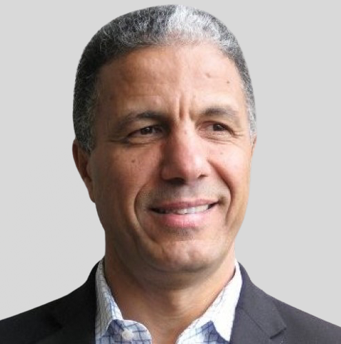
Habib Hichri, Ph.D.
Ajinomoto Fine-Techno Corporation USA
Education:
Experience:
Habib Hichri is an Executive Vice President, Senior Fellow Global Applications and Business Development at Ajinomoto Fine-Techno Corporation USA. Prior to joining AFT USA, Habib was Director of Applications Engineering at SUSS MicroTec Photonics Systems USA where he provided patterning solutions for advanced semiconductors packaging customers. Before joining SUSS MicroTec, Habib spent about 12 years with IBM Semiconductors Research and Development Center (IBM SRDC) in East Fishkill, NY where he worked as lead process integration engineer for microprocessor (IBM), games and communications chips. He later was promoted to management positions within IBM on process development in the front end of line area for microprocessor fabrication. Habib holds over 40 U.S. patents and authored over 75 publications and presentations and a book chapter in “Advances in Embedded and Fan-Out Wafer Level Packaging Technologies” (Wiley – IEEE) first Edition. Habib received Master and PhD degrees in Chemical Engineering from the Claude Bernard University at Lyon, France, and an MBA degree from the State University of New York at Buffalo. Habib is the chair of the Orange County California IEEE/Electronic Packaging Society (EPS) Chapter. He is also a member of the technical committees of Electronic Components and Technology Conference (ECTC), International Microelectronics Assembly and Packaging Society (IMAPS). He was the general chair of IMPAS 2020. Habib is IMAPS Society Fellow. He is currently member of the IMAPS executive council. Habib is Board member of International Electronics Manufacturing Initiative (iNEMI) since April 2024 and International Semiconductor Industry Group (ISIG) since April 2025.
Company Profile
Ajinomoto Fine-Techno Co., Inc. (AFT) is a subsidiary of the Ajinomoto Group responsible for the fine chemicals division. AFT (est. 1942) continues to deliver materials that can suit a wide range of customer needs in our four main strengths: molecular design, formulation, process development, and solutions. Our customers have commended us for our electronic materials. We have grown to play a major part in their value chains for electronics, automotive, and a variety of other products. We continue to refine our ability in materials science through research and development to continue creating value with our customers. We strive to provide the highest quality products, services, and information for our customers. Beyond our Ajinomoto Build-up film®, we’ve expanded our material portfolio to include molding, photo dielectric, magnetic, and optoelectronics. To maintain our leadership in our specified industry, we are devoted to providing state-of-the-art material, technology know-how, and customer service.
Company Products & Services
Please visit the website: Product information – Ajinomoto Fine-Techno Co.,Inc. (aft-website.com)

09:45 – 10:10
Joint Case Study: Powering Electronics with Active and Passive Devices
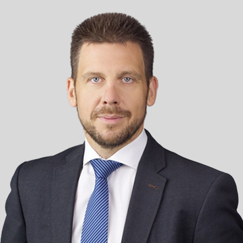
Ole Gerkensmeyer
Nexperia
Ole Gerkensmeyer is VP Sales EMEA at Nexperia, a leading semiconductor manufacturer for essential and power semiconductors. He started his semiconductor career over 25y ago with Texas Instruments, where he held several management positions over his 17year tenure. He then became General Manager of Future Electronics’ distribution business in Central Europe. Most recently, he spend over 5 years with Wolfspeed, where he not only led their EMEA Automotive business but also was influencial in establishing corporate business development projects. – Next to Nexperia, Ole is also active as an advisory board member at the world’s power electronics conference: PCIM. His interest is focussed on semiconductor business growth as well as power electronics.
Company Profile
Headquartered in the Netherlands, Nexperia is a global semiconductor company with a rich European history and over 15,000 employees across Europe, Asia, and the United States. As a leading expert in the development and production of essential semiconductors, Nexperia’s components enable the basic functionality of virtually every electronic design in the world – from automotive and industrial to mobile and consumer applications.
The company serves a global customer base, shipping more than 100 billion products annually. These products are recognized as benchmarks in efficiency – in process, size, power, and performance. Nexperia’s commitment to innovation, efficiency and stringent industry requirements are evident in its extensive IP portfolio, its expanding product range, and its certification to IATF 16949, ISO 9001, ISO 14001 and ISO 45001 standards.


Sherin Ahmed El-Badry Sadek, Ph.D.
Würth Elektronik
Dr. Sherin Ahmed El-Badry Sadek is a multilingual expert in international relations and strategic partnerships, currently Strategic Partnership Manager EMEA at Würth Elektronik in Munich. She holds a Ph.D. in Educational Sciences and a Master’s in Advanced European and International Studies. Her career emphasizes engagement with the Middle East, including leading partnership development for a new Egyptian-European University in Cairo and diplomatic roles in Berlin and Qatar. Dr. Sadek’s experience in building institutional alliances, driving innovation projects, and her proficiency in seven languages enable her to operate effectively in complex, intercultural environments.
Company Profile
Würth Elektronik eiSos Group is a manufacturer of electronic and electromechanical components for the electronics industry and a technology company that spearheads pioneering electronic solutions. Würth Elektronik eiSos is one of the largest European manufacturers of passive components and is active in 50 countries. Production sites in Europe, Asia and North America supply a growing number of customers worldwide.
The product range includes passive components, power modules, digital isolators, optoelectronics, electromechanical components, thermal management solutions, sensors and wireless modules. The portfolio is rounded off by customer-specific solutions.
The unrivaled service orientation of the company is characterized by the availability of all catalog components from stock without minimum order quantity, free samples and extensive support through technical sales staff and selection tools.
Würth Elektronik is part of the Würth Group, the global market leader in the development, production, and sale of fastening and assembly materials, and employs around 7,500 people. In 2024, the Würth Elektronik Group generated sales of 1.02 Billion Euro.
Würth Elektronik: more than you expect! Further information at www.we-online.com

10:15 – 10:30
MEMS and Sensors for the Next-Gen Edge

Eric Aguilar
Omnitron Sensors
An award-winning entrepreneur, Eric Aguilar is a visionary leader in the field of advanced sensor systems for complex systems, such as robotics and autonomous platforms.
Throughout his distinguished two-decade career, Eric’s passion for sensor design and innovation has made him a key player in the industry. His expertise includes leading teams at renowned companies such as Tesla, where he managed a crew of 300 engineers on the firmware for Model 3, and at X, where he spearheaded the development of Google Project Wing, an autonomous drone delivery service.
Eric’s expertise in sensor integration includes leadership positions at autonomous vehicle and robotics companies. His role in steering product development for a sensor company later acquired by Google — as well as for his pioneering work building sensors for drones at US Navy Research Labs — further showcases his depth of experience.
Eric earned a BS in Electrical Engineering from California State Polytechnic University and has pursued advanced studies in Electrical and Electronics Engineering at the University of Southern California. His work continues to shape the future of MEMS and sensor technology, making him a sought-after thought leader and speaker in the field.
Company Profile
Omnitron Sensors is rewriting the script on building high-performance low-cost sensors for the world of tomorrow. Leveraging its executive team’s extensive experience designing, fabricating, and using MEMS sensors, Omnitron has developed a “new topology for MEMS” that addresses some of the most pressing pain points in MEMS manufacturing.
Featuring the clever arrangement of silicon process steps and a new packaging method, Omnitron’s topology significantly improves performance to produce robust, rugged, reliable, repeatable, and low-cost MEMS sensors in high volumes by leveraging commercial MEMS foundries.
The company’s first proof point of its new topology for MEMS is a large, robust, low-cost, MEMS scanning mirror for long-range LiDAR.

10:30 – 11:30
Networking Break & Business Meetings 5&6
11:35 – 11:50
MEMS Driving Smart Systems from Europe to MENA

Anton Hofmeister
STMicroelectronics
Anton Hofmeister is Group Vice President and General Manager of R&D in ST’s Analog, Power & Discrete, MEMS & Sensors Group. He is also Managing Director of ST’s German subsidiary since 2016.
Hofmeister joined Thomson Semiconductors (a predecessor company to STMicroelectronics) as a marketing engineer in 1986. He subsequently held management positions in product marketing, key account management and corporate strategic marketing. In 1997, Hofmeister was appointed Director of a System R&D team in San Diego, USA, and became subsequently Director of the Print Head Business Unit. In 2005, he was appointed General Manager of the Microfluidics Division and has broadened his responsibility with the MEMS Microactuator Division in 2015, managing the MEMS business for a variety of applications in Consumer Electronics, Automotive, Industrial, and Medical markets.
Hofmeister has served as a board member of the Singapore-based Molecular Diagnostics company Veredus Laboratories. He is currently a member of the Governing Council of the MEMS&Sensor Industry Group (MSIG) at SEMI and a board member of the European Association on Smart Systems Integration (EPoSS).
Anton Hofmeister was born in Munich and graduated with a Master’s degree in Engineering from the University of Munich.
Company Profile
At ST, we are more than 50,000 creators and makers of semiconductor technologies mastering the semiconductor supply chain with state-of-the-art manufacturing facilities. An integrated device manufacturer, we work with more than 200,000 customers and thousands of partners to design and build products, solutions, and ecosystems that address their challenges and opportunities, and the need to support a more sustainable world. Our technologies enable smarter mobility, more efficient power and energy management, and the wide-scale deployment of cloud-connected autonomous things. We are committed to achieving our goal to become carbon neutral on scope 1 and 2 and partially scope 3 by 2027. Further information can be found at www.st.com.

11:55 – 12:10
Transforming Challenges into Opportunities: The Journey of the First Saudi Fab
When we first set out to build Saudi Arabia’s first semiconductor fab, we faced significant challenges: limited supply chains, a shortage of local talent, and few academic programs in the field. But rather than seeing these as obstacles, we saw them as opportunities. We partnered with universities to develop new programs, provide training and internships, and build the skills needed for a thriving semiconductor workforce. Today, our company is not only helping shape a robust local ecosystem but also serving as the bridge between international technology leaders and the Kingdom, driving innovation and empowering the next generation of talent.
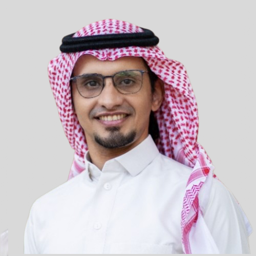
Abdullah Alshehri, Ph.D.
Saudi Electronic Materials Company
Dr. Abdullah earned his undergraduate degree from the University of Brighton and pursued both his Master’s and PhD at King Abdullah University of Science and Technology (KAUST), specializing in circuit design and developing low-power, high-performance ASICs for MEMS sensors. He is currently an Assistant Professor at Umm Al Qura University and serves on the KAUST Saudi Alumni Executive Committee. Dr. Abdullah has authored and co-authored more than 10 research papers, co-founded TRYSL Tech and DeepCARES, and leads the Business Development Unit at the Saudi Electronics Material Company, with professional experience collaborating with Aramco, STC, and Cadence.
Company Profile
The Saudi Electronic Materials Company (SEMC) is a pioneering semiconductor company driving innovation across Saudi Arabia, the MENA region, and beyond. With expertise in MEMS and infrared (IR) technologies, we deliver end-to-end solutions covering design, fabrication, packaging, and testing.
Equipped with a state-of-the-art cleanroom and advanced facilities, SEMC works alongside leading global research institutions and equipment providers to shape the next generation of semiconductor technologies that support national priorities and meet international standards.
Guided by Saudi Vision 2030, we are building a sustainable semiconductor ecosystem that fuels innovation, accelerates industrial growth, and strengthens the Kingdom’s role as a competitive force in the global semiconductor industry.
Company Products & Services
12:15 – 12:30
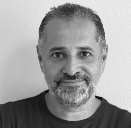
Mo Maghsoudnia
UltraSense Systems
Mo Maghsoudnia is the visionary Founder and dedicated CEO at the helm of UltraSense Systems, a pioneering company in the technology and manufacturing sector. With a track record of transformative leadership and innovation, Mo has been instrumental in shaping the industry landscape.
Before founding UltraSense, Mo Maghsoudnia made significant contributions as the Vice President of Technology & Manufacturing at InvenSense. In this influential role, he oversaw global operations and spearheaded the development of cutting-edge Process Technology. Under his guidance, InvenSense achieved remarkable success, culminating in its acquisition by TDK for a staggering $1.4 billion in 2017.
Prior to his tenure at InvenSense, Mo Maghsoudnia served as the Vice President of Manufacturing at NetLogic MicroSystems. Here, he demonstrated his exceptional ability to steer manufacturing operations, elevating the company from a single product line to a diversified product portfolio powerhouse. His adept leadership, combined with a diverse product range, paved the way for Broadcom’s acquisition of NetLogic MicroSystems for a
remarkable $4 billion in 2012.
Mo’s expertise is firmly rooted in his academic pursuits, holding a Master of Science in Electrical Engineering from Santa Clara University. His passion for innovation is further underscored by his impressive intellectual property portfolio, boasting 12 patents, and an extensive list of research papers that he has authored.
Mo Maghsoudnia’s unwavering commitment to technological advancement and his exceptional leadership have left an indelible mark on the tech and manufacturing sectors, solidifying his status as a true industry luminary.
Company Profile
UltraSense Systems is pioneering the next generation of human–machine interface intelligence, built on its proprietary ultrasound and piezoelectric platform that fuses sensing, haptics, and edge processing into compact, solid-state systems. Its multimodal sensor-fusion architecture—integrating touch, force, ultrasound, lighting, and haptic feedback—creates a unified tactile interface layer that transforms how users interact with devices and environments. The company’s silicon and systems portfolio enables software-defined smart surfaces that operate across diverse materials and form factors, delivering the responsiveness, precision, and design freedom demanded by advanced mobility and next-generation consumer electronics. In automotive, UltraSense Systems powers intelligent cabin interfaces that integrate sensing, actuation, and illumination into seamless surfaces for a futuristic in-cabin experience. In high-end consumer devices, including smartphones and AR glasses, its solutions enable thinner, more immersive, and spatially aware user experiences. Built on deep expertise in ultrasound physics, MEMS, and mixed-signal ASIC design, UltraSense Systems is extending its technology platform into new domains where tactile perception and spatial awareness will define the next era of user experience—combining precision sensing, embedded intelligence, and solid-state reliability to bridge the physical and digital worlds. For more information, visit www.UltraSenseSystems.com.
Company Products & Services
UltraSense Systems delivers the most advanced solid-state HMI technology for the next generation of user interfaces. Our TouchPoint™ family of silicon controllers integrates multi-modal sensing — ultrasound, capacitive, and piezoelectric — with lighting, haptic feedback, and on-chip intelligence.
From TouchPoint C (CapForce™) to Z (UltraForce™), Q (TapForce™), and Edge, each device fuses sensing, control, and communication into a single SoC — enabling touch and force interaction through metal, glass, fabric, and composite surfaces.
Complemented by our UltraSwitch™, UltraSlide™, and UltraTouch™ system modules, UltraSense provides a full-stack platform that transforms static surfaces into intelligent, software-defined interfaces — powering the future of automotive, AR glasses, and high-end consumer devices.
UltraSense Systems — The Future of Solid-State HMI
| Layer | Offering | Description |
| Silicon Platform | TouchPoint™ HMI Controllers | Multi-mode SoCs integrating touch + force sensing, lighting, haptics, and AI-based algorithms |
| C – CapForce™ | Capacitive + Force sensing controller | |
| Z – UltraForce™ | Ultrasound + Force sensing controller | |
| Q – TapForce™ | Piezoelectric Force sensing controller | |
| Edge – Cluster/Slider | Multi-channel HMI SoC with Neural Touch Engine™ + LIN | |
| System Modules | UltraSwitch™ / UltraSlide™ / UltraTouch™ | Complete smart-surface solutions integrating sensing, feedback, and lighting |
| Applications | Automotive • AR Glasses • Consumer Devices | Solid-state, software-defined interfaces that modernize the user experience |

12:55 – 13:05
Electrification, Sustainable Smart Infrastructure
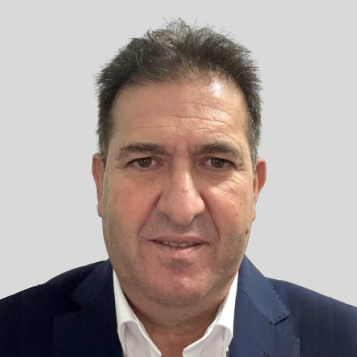
Kamel Ait Mahiout
ZCE ( Zero Carbon Emission)
Over 35 years in Semiconductor and high-tech industry,
President & CEO ZCE Group Energy Innovation & Decarbonation
President & CEO Novasensing, Neuromorphic ML/AI Edge AI company
President of International Semiconductor Executive Summits as of end on June 2024.
ATLANT3D as a CCO, ALD Process direct deposition,
Worked at Applied Material on the advance packaging corporate business on Hybrid bonding Cluster, Digital Lithography and Metrology & Inspection.
Prior to AMAT he served as CEO of Unity SC, inspection, and Metrology company where he reengineered the company from the product and organization to alignment with tiers 1 customers,
Prior to Unity, Kamel Served Amkor Technology as a President and General manager for Europe & Singapore over 18 years aligning and growing the company with European key players and starts up.
Started in the industry over 35 years ago as RF and Microwave R&D Engineer designing product & Modules for Aerospace, Military, and telecom markets, then served managing internal and external Operations Front end and Back end.
Kamel holds a Bachelor in Electronics from University HB in Algeria and a master’s in electronic from Reims University France.
Company Profile
WATTELZCE® by ZCE
Registered Trademark | BPI Deeptech | JEI (Jeune Entreprise Innovante)
Patented Technological Solutions: FR2508679, FR2510175
About Us
WATTELZCE® by ZCE is a pioneering Deeptech company recognized by BPI France for its breakthrough innovations in sustainable energy and electric mobility. As a JEI (Young Innovative Company), we are committed to developing smart, secure, and shareable charging infrastructure designed to make electric mobility accessible to all.
Our patented solutions and connected ecosystem bridge the gap between technology, sustainability, and accessibility — turning every power outlet into a smart charging station
Vision
To become the “AirBnB of electric charging,” transforming every outlet into a smart, secure, and sharable charging station.
Mission
To make electric mobility accessible, convenient, reliable, and equitable everywhere, while reducing carbon emissions and promoting clean energy adoption.
Company Products & Services
13:10 – 13:20
Revolutionizing Silicon Carbide Substrate Polishing via Environmentally-Conscious Slurry and Tool Designs
Standard SiC polishing processes employ aggressive, environmentally harmful redox chemistries containing potassium permanganate to achieve acceptable polishing outcomes. Polisher wear and tear caused by such an aggressive chemical remains a significant concern. Instead, we have chosen a two-pronged approach to improve SiC polish. Firstly, we have patented a hydrogen peroxide-based SiC slurry containing alumina nanoparticles and aspartic acid complexes for final polishing. The second approach utilizes a novel polisher that we have designed, are now manufacturing, and are selling worldwide. We call our invention CARE-TEC® or “CAtalyst-Referred Etching Technology”. The technology employs a polymeric pad onto which a catalytic platinum or ruthenium film is sputtered. With pH-adjusted water as the slurry substitute, an electric potential is applied to the SiC substrate and the pad. The principal mechanism of polishing SiC is the continuous etching of the substrate by catalytically converting the top layers of SiC into monolayers of silicon dioxide, which are then removed mechanically (via polishing) at moderate pressures.

Ara Philipossian, Ph.D.
Araca
Dr. Ara Philipossian has been a professor of Chemical Engineering at the University of Arizona since 2001, where he holds the Koshiyama Chair of Planarization. Since its establishment in 2004, he has also been the Co-Founder, President, and CEO of Araca Incorporated, the premier provider of services and equipment to the polishing and planarization industry worldwide. He received his BS, MS, and PhD in Chemical Engineering from Tufts University in 1983, 1985, and 1992, respectively. From 1992 to 2001, he was the Materials Technology Manager at Intel Corporation (Santa Clara, CA, USA), responsible for the development, characterization, implementation, and sustaining of new and existing CMP and post-CMP cleaning consumables, low-k dielectrics, and electroplating chemicals. From 1986 to 1992, he worked at Digital Equipment Corporation (Hudson, MA, USA) as a process development manager focusing on thermal silicon oxidation, diffusion, LPCVD of dielectric and gate electrodes, and wafer cleaning technology. Dr. Philipossian has authored approximately 180 archival journal publications and 210 conference proceedings articles. He holds 36 patents in semiconductor processing and device fabrication.
Company Profile
Founded in 2004 and headquartered in Tucson, AZ (USA), Araca Inc. provides unique, enabling, and fully customized solutions to our clients in IC planarization and semiconductor polishing for silicon and wide band-gap material applications. Clients include leading IC makers, consumables suppliers, OEMs, universities, and research centers. Our products lower the cost of ownership (COO) of CMP or polishing modules, allowing clients to save money and preserve the environment by reducing slurry and rinse water consumption, increasing pad and diamond disc life, while increasing polisher availability, throughput, and yield.
Company Products & Services
Our key equipment add-on products, namely, Flucto-CMP®, ESE-100® and the Slurry Injection System (SIS®) are compatible with all polishers. SIS® continues to be rapidly adopted in HVM due to its proven COO and environmental benefits, while Flucto-CMP® is undergoing extensive beta-testing at multiple major OEMs. We provide sensorized and affordable polishers-tribometers and PVA brush scrubbers-tribometers (up to 300 mm wafers), which offer significant reductions in process and consumables characterization costs and R&D expenses. CARE-TEC® is our revolutionary SiC and GaN final polishing system; it requires no slurry or conditioning disc. In our brand-new Class 100 clean room at the University of Arizona, we provide research and foundry services for all sizes and types of substrates. We perform high-quality and highly scientific analytical and functional tests on pads, slurries, conditioners, retaining rings, brushes, and cleaning chemicals. Our pad surface preparation and grooving services are second to none. We develop customized CMP, polishing, and cleaning consumables and processes for various applications, including SiC and GaN, and remain open to co-development programs. We also offer delayering services for 3D NAND and DRAM structures for diagnostics.

13:20 – 14:15
Networking Lunch
14:20 – 14:35
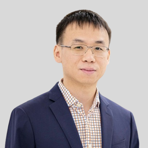
Xiaohang Li
King Abdullah University of Science and Technology (KAUST)
Company Profile
KAUST is a world-class research university in the world. It has ranked No. 1 in the Times Higher Education Arab University Ranking since 2023. In the semiconductor area, KAUST has amassed the largest cluster of top-notched researchers and entrepreneurs in MENA and operated state-of-the-art nanofabrication and characterization facilities. Through research, innovation, entrepreneurship activities as well as numerous alumni it has trained, KAUST has been a pioneer and catalyst of the semiconductor ecosystem in Saudi Arabia and MENA region.
Company Products & Services
Education, training, research, innovation, entrepreneurship, consulting.
14:40 – 14:55
Mohssen Moridi, Ph.D.
Silicon Austria Labs (SAL)
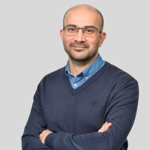
Dr. Mohssen Moridi is an expert in microtechnology with over 20 years of experience in the development of MEMS devices. He holds a Master’s and Ph.D. in Microtechnology from École Polytechnique Fédérale de Lausanne (EPFL), Switzerland. After completing his doctoral studies, he held various research positions in Switzerland, contributing to advancements in microsystems technology. In 2016, he moved to Austria to lead the Microsystem Division at CTR AG, where he established a MEMS department and managed the development of a new cleanroom dedicated to industrial R&D. Since 2019, he has been part of Silicon Austria Labs (SAL) and currently serves as Senior Executive Director and Head of the Microsystems Research Division. In this role, he leads a team of over 60 researchers, driving innovation in thin-film technologies, integrated photonics, and magnetic and piezoelectric microsystems. With extensive experience at the intersection of research and industry, Dr. Moridi plays a key role in shaping cutting-edge microsystem technologies, bridging fundamental research with industrial applications.
Company Profile
Silicon Austria Labs (SAL) has been founded to be a top European research center for electronic-based systems. In the network of science and economy, we carry out research at a global level and create the basis of groundbreaking products and processes.

15:00 – 15:15
Oleh Krutko, Ph.D.
imec
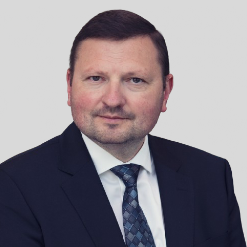
Oleh Krutko is a Senior Vice President of Design and Systems R&D at imec. In this role, he leads global research and engineering organization responsible for developing systems and circuits IP and solutions as well as managing ASIC volume production operations. Previously he was a General Manager of IC-Link by imec, imec division that offers ASIC solution development and manufacturing services.
Prior to joining imec, Oleh Krutko was a Senior Director of Engineering at AMD, managing Analog and Digital RF organization responsible for developing SOCs and ASICs for wireless infrastructure, defense, aerospace, test, and measurement applications. Previously, he was a Director of Engineering at Qorvo Texas, where he was responsible for RF, millimeter wave, broadband and power product development organization, and RF Design Specialist at Nokia North America R&D, where he was working on high efficiency power amplifiers and transmitters for wireless infrastructure.
Oleh Krutko has PhD in Electrical Engineering from the University of Cincinnati, Ohio, USA. He co-authored 40 journal and conference papers and has 7 patents. Oleh Krutko is a senior member of IEEE and Technical Program Committee member of IEEE RFIC conference.
Company Profile
Imec is a world-leading research and innovation center in nanoelectronics and digital technologies. Imec leverages its state-of-the-art R&D infrastructure and its team of more than 5,500 employees and top researchers, for R&D in advanced semiconductor and system scaling, silicon photonics, artificial intelligence, beyond 5G communications and sensing technologies, and in application domains such as health and life sciences, mobility, industry 4.0, agrofood, smart cities, sustainable energy, education, … Imec unites world-industry leaders across the semiconductor value chain, Flanders-based and international tech, pharma, medical and ICT companies, start-ups, and academia and knowledge centers. Imec is headquartered in Leuven (Belgium), and has research sites across Belgium, in the Netherlands and the USA, and representation in 3 continents. In 2021, imec’s revenue (P&L) totaled 732 million euro.
Further information on imec can be found at www.imec-int.com.
15:20 – 15:35

Karim Hamzaoui
Preferred Networks
Company Profile
Preferred Networks (PFN) is a leading Japanese AI technology company known for its vertically integrated development of cutting-edge technologies—from custom AI chips, generative AI foundation models to real-world AI solutions and products. PFN plays a key role in advancing Japan’s AI sovereignty and has earned a strong domestic reputation. PFN’s AI solutions span across diverse industries including manufacturing, materials, energy, pharmaceuticals, healthcare, finance, retail, and entertainment. The company is currently developing a novel AI inference chip, leveraging its highly energy-efficient MN-Core™ logic and a new memory technology, with a release targeted for early 2027.
Company Products & Services
Preferred Networks (PFN) develops cutting-edge technologies across the AI value chain from semiconductors, supercomputers, generative AI foundation models to AI solutions and products:
MN-Core™ — a series of highly energy-efficient AI chips, which made a debut topping the Green500 list of the world’s most energy-efficient supercomputers three times in 2020/21. PFN is currently developing a new line of MN-Core chips focused on AI inference, set for release in early 2027.
Preferred Computing Platform™ (PFCP™︎) — a cloud-based service that provides users with access to the computing power of MN-Core 2. PFN has also announced a joint venture with Mitsubishi Corporation and IIJ aiming to launch an MN-Core™-based IaaS commercial service in 2026.
PLaMo™ — a series of Large Language Models developed fully from scratch by PFN, delivering top-tier performance in Japanese-language capabilities. These models power a wide range of AI applications in sectors such as finance, healthcare, and the public sector.
Matlantis™ — a cloud-based, high-speed universal atomistic simulator. Powered by a machine learning interatomic potential (MLIP), Matlantis significantly accelerates the simulation workflow in new materials discovery across industries such as semiconductor, automotive, and energy, by bypassing traditional heavy electronic state calculations.

16:00 – 16:15

Sam Bordbar
Cadence
Sam Bordbar is a Sr Account Technical Executive with nearly three decades of experience shaping the semiconductor and electronic design automation (EDA) landscape. His career spans the full evolution of digital back-end design, from the early days of EDA to today’s advanced multi-die architectures, that gives him a unique view on the industry’s transformation.
As a recognized Implementation Solutions Leader and a key member of the Global Account Management team, Sam has driven strategic partnerships and delivered implementation excellence across Semiconductor, AI, Cloud, and Data Center ecosystems. In his current role at Cadence, he leads business development and strategic initiatives across the Middle East, helping customers on rapidly evolving technology areas.
Sam holds a BS in Electronic and Computer Engineering from the KTH Royal Institute of Technology in Stockholm. His blend of technical depth and practical industry insight, developed over 26 years in EDA, makes him an influential voice in conversations about the future of semiconductor design.
Company Profile
Cadence is a market leader in AI and digital twins, pioneering the application of computational software to accelerate innovation in the engineering design of silicon to systems. Our design solutions, based on Cadence’s Intelligent System Design™ strategy, are essential for the world’s leading semiconductor and systems companies to build their next-generation products from chips to full electromechanical systems that serve a wide range of markets, including hyperscale computing, mobile communications, automotive, aerospace, industrial, life sciences and robotics.

16:15 – 16:45
Networking Break & Business Meetings 7&8
16:50 – 17:05

Ahmed Alfaifi
National Semiconductor Hub Saudi Arabia

17:10 – 17:40
Panel Discussion: China-Middle East Semiconductor Supply Chain Complementarity: From Technology Export to Localized Collaboration
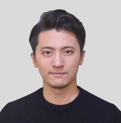
Moderator
Tong Wu, Ph.D.
onsemi
吴桐,安森美(onsemi)中国区汽车市场负责人,上海交通大学半导体物理专业,数学专业辅修本科毕业,美国田纳西大学电气工程博士学位。吴博士在半导体封装,碳化硅设计应用方面拥有 10 余年的研发和工业经验。 目前在安森美负责中国区汽车技术与市场,覆盖产品设计,制造,市场及应用,了解新能源行业的市场、供应链、开发流程以及解决方案。与国内多家车厂、Tier 1 保持着深度合作以及技术支持。曾就职于美国田纳西州橡树岭橡树岭国家实验室(ORNL),以及车厂研发团队,共在国际会议和期刊上发表了 40 多篇论文,同时获得了多项 半导体方面的美国专利。
Dr. Tong Wu is onsemi SiC Expert & Leader of China Auto Marketing & Technical Team, responsible for developing the SiC market in China, as well as providing technical support for car OEMs and Tier1s, and participating in multiple NPIs. He has more than 10 years of R&D and industrial experience in wide band-gap devices and its applications. Prior to joining onsemi, Dr. Wu conducted his research at Oak Ridge National Laboratory(ORNL) for multiple DOE-funded SiC-related projects.
Dr. Wu received his B.S. degree from Shanghai Jiao Tong University, majoring in semiconductor physics and minoring in mathematics. Dr. Wu received his Ph.D. in Power Electronics from the University of Tennessee, USA. He conducted his doctoral research at the Power Electronics and Electric Machinery Research Center of Oak Ridge National Laboratory(ORNL). Dr. Wu has authored/co-authored more than 40 papers in international conferences and journals and awarded several U.S. patents in SiC area.
Company Profile
onsemi (Nasdaq: ON) is driving disruptive innovations to help build a better future. With a focus on automotive and industrial end-markets, the company is accelerating change in megatrends such as vehicle electrification and safety, sustainable energy grids, industrial automation, and 5G and cloud infrastructure. With a highly differentiated and innovative product portfolio, onsemi creates intelligent power and sensing technologies that solve the world’s most complex challenges and leads the way in creating a safer, cleaner, and smarter world.


Panelist
Xiaoming Wu
Chipright

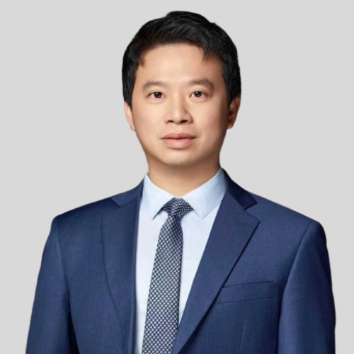
Panelist
Bingan Chen
Naso Tech
Company Profile
Naso Tech founded in 2018, has been focused on designing and manufacturing high-end equipment for advanced materials. Our core team members are from University of Cambridge and well- known industry firms, who bring strong and wealth of expertise to the company.
We are experienced in the field of advanced semiconductor manufacturing equipment, including chemical vapor deposition (CVD), metal organic chemical vapor deposition (MOCVD), Atomic Layer Deposition(ALD) and ETCH(etching).
Company Products & Services
CVD:NASO TECH’s SiC Epitaxial Reactor is a specialized equipment designed for the epitaxial layer growth—a core process in silicon carbide chip production. This step is critical for manufacturing diodes and power semiconductor devices.
PVD:NASO TECH’s PVD Equipment primarily deposits various metallic and non-metallic thin films on wafer surfaces during semiconductor fabrication. It plays a key role in forming essential conductive pathways, electrode contacts, and protective barriers or integrated circuits.
ALD:NASO TECH’s ALD System is used in perovskite solar cell manufacturing for depositing high-quality functional layers with extreme uniformity and conformity—such as electron transport layers (ETL) and interface passivation layers. It addresses critical challenges in cell stability and efficienc.

Panelist
Wilson Hong
Wuxi Leapers Semiconductor Co., Ltd.
Wilson Hong, Chair of ISIG China, Partner and CTO of Wuxi Leapers Semiconductor. He has 20 years R&D experience on power electronic engineering, software engineering, electric drive system and high voltage architecture in EV.
He used to be senior director in NIO, built the power electronic and software team from 1 person in 2015 to ~200 people in 2023. He led the team to deliver over 1.6 million inverters with several classes and different semiconductors, incl. first highest NEDC efficiency SiC Inverter, first 3-in-1 240kW IM system, first 3-in-1 160kW PM system and 4-in-1 HV ECU.
He hold over 50 power electronic, software, electric drive system patents cross China, US and EU. He won the first Prize and second Prize of Science and Technology Progress of China Association of Automobile Manufacturers in 2021 and 2024.
He is now working on power module advanced packaging, super charging and AI power.
Company Profile
Wuxi Leapers Semiconductor Co., Ltd. brings together experienced professionals at home and abroad, including wafer process and device design, module packaging design, product application, marketing and product operation. Major products include high-reliability SiC and IGBT modules for new energy vehicles and industrial applications. Products are used in new energy vehicles, smart grids, renewable energy, industrial motor drives, medical equipment, power supplies and other scenarios and fields; the company is headquartered in Wuxi, China, and has a research and development center in Japan.We adopts innovative packaging materials and processing technology to provide complete module application solutions for the miniaturization, efficiency and light weight of electric drive systems and inverters for new energy vehicles. Meet the needs of high-performance, high-reliability new energy vehicles and high-end industrial power semiconductor modules.

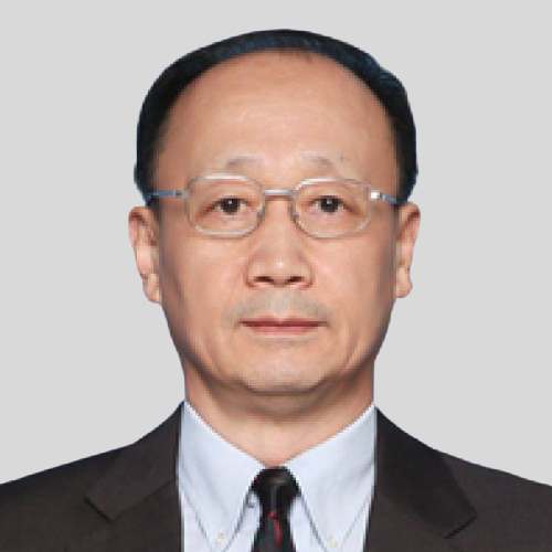
Panelist
SYNLINX Seminconductor Super Incubator
Allan Zhou holds a Ph.D. in Chemistry and Materials Science from the University of Connecticut, USA.
He has served as CEO of Shanghai GTA Semiconductor Co., Ltd., Professor at Fudan University, Distinguished Professor and Adjunct Dean of the School of Excellence in Engineering at Shanghai Dian Ji University, Senior R&D Scientist at Applied Materials Inc. (USA), as well as Senior R&D Manager, Fab Director of Large-Scale Manufacturing, and Senior Director of the Operations Center at Semiconductor Manufacturing International Corporation (SMIC).
With extensive expertise in the engineering principles and methodologies of large-scale production for semiconductor micro-nano devices, he has dedicated his career to the research, development, and industrialization of intelligent manufacturing equipment and materials for semiconductor micro-nano devices—particularly focusing on the large-scale industrialization of domestic semiconductor equipment and materials in China. He is recognized as one of the key pioneers in the large-scale industrialization of copper interconnect technology for semiconductor integrated circuits in China.
He has been awarded the 1st Level Prize of the Shanghai Science and Technology Progress Award, published over 20 academic papers, and holds 21 international patents.
He has been selected as a National and Shanghai Distinguished Expert (Innovation Category), honored as an Outstanding Entrepreneur of the Year by China Electronics Corporation (CEC), and received the inaugural Shanghai Outstanding Talent Award.

Panelist
Weiping (Bill) Li, Ph.D.
Weiping Li is a seasoned executive in the semiconductor and IT industry with vast experience both in the US and China. He founded Yibu Semiconductor in 2020 that pioneered Si bridge chiplet packaging in China. Prior to that, he served as the Senior Vice President with Unigroup and was the Chairman of the Board of its subsidiary, Unimos. He was Vice President of Jiangsu Changjiang Electronics Technolgy (JCET) for 8 years before Unigroup. He also worked in the US at Amkor, Motorola SPS and Delphi Delco in R&D and product management roles.
Weiping Li held a Ph.D. degree from Georgia Institute of Technology in Materials Science and Engineering. He received the “Extinguished Alumni in Engineering Award” from the same school in 2012. He has over one hundred of patents and numerous technical and industrial publications/talks in electronics packaging.
17:40 – 18:00
Closing Remarks
End of content
End of content