9-11 December 2025
Muscat, Oman
No posts
4-5 September 2025 - Dresden


07:30 – 08:30
Registration
08:30 – 08:45
M.S.W.S. & I.S.I.G. Welcome
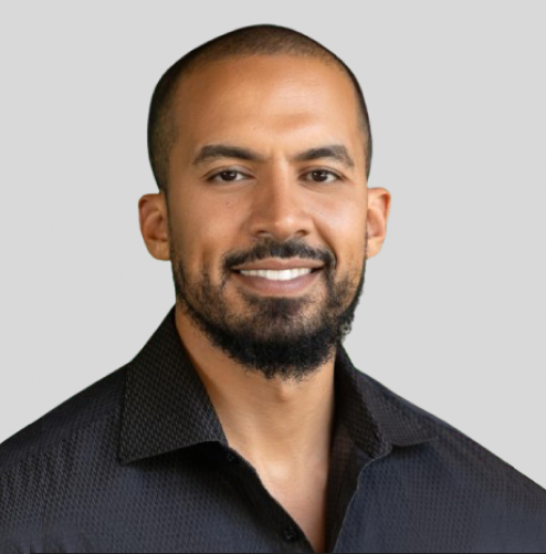
Salah Nasri
International Semiconductor Industry Group (ISIG)
Salah Nasri is the CEO and Co-Founder of the International Semiconductor Industry Group (ISIG), a global organization founded in 2010 that connects and empowers semiconductor decision-makers through strategic leadership platforms, executive summits, and collaborative initiatives. ISIG has become a trusted global hub for industry leaders driving innovation and progress across the semiconductor value chain.
With extensive experience across the semiconductor sector, Salah has played a pivotal role in fostering global collaboration among industry leaders. Under his leadership, ISIG has evolved into one of the most influential communities in the semiconductor ecosystem—bringing together executives, innovators, and policymakers across regions including the United States, Europe, Asia, and the Middle East.
Salah has been instrumental in expanding ISIG’s reach and impact, curating high-level summits and initiatives that drive dialogue and progress across critical areas such as semiconductor manufacturing, AI, MEMS, automotive electronics, and advanced packaging. His vision continues to position ISIG as a key platform for thought leadership, networking, and strategic industry alignment.
Earlier in his career, Salah held positions at Credit Suisse, Goldman Sachs, Worldwide Business Research, and the International Business Development Group. He studied International Relations and Economics at Oxford University and Loughborough University, and in 2024 became a Stanford University alumnus after completing the Stanford Executive Program. In addition to his role at ISIG, Salah also serves on the Advisory Board of Atlant3D, a pioneer in atomic-layer advanced manufacturing solutions.
Company Profile
Established in 2010, the International SemiconductorIndustry (I.S.I.G.) is a prestigious & trusted associationwithin the semiconductor industry, renowned fororchestrating major regional summits across the globe,ranging from the U.S, the Middle East & Asia via ourdivision, the International Semiconductor ExecutiveSummits (I.S.E.S.). Our summits are fully endorsed bylocal governments and leading companies in all areas ofthe semiconductor supply chain.
Moreover, I.S.E.S. serves as the Premier platform for senior executives in technology, manufacturing, and R&D from diverse semiconductor companies, technology providers, and affiliated industries.
Our events are instrumental helping to shed light onto key industry trends, drive innovation and influence key decisions to help shape, and advance the growth of the semiconductor sector.
08:50 – 09:10
Keynote
MEMS-based Laser Scanning Displays for Augmented Reality
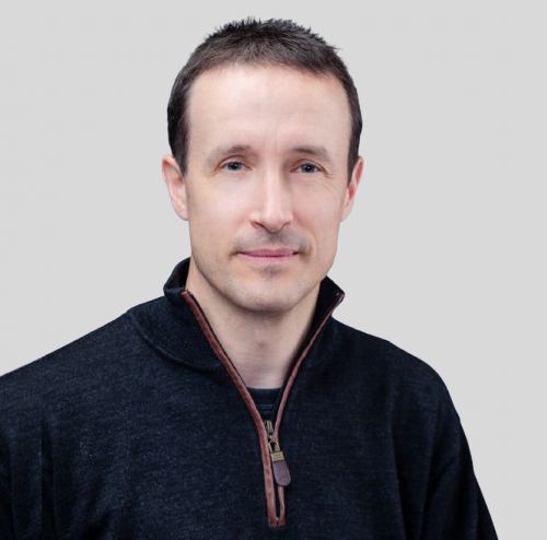
Ken Diest
Meta
Ken Diest is a Research Manager and Tech Lead at Meta’s Reality Labs, where he leads programs focused on MEMS and micro-actuator technologies. His focus is on developing these technologies from early stage through production to address critical opto-mechanical and display challenges in AR/MR.
A Materials Scientist by training, Ken’s prior work focused on tunable devices and materials with an emphasis on optical systems. He was the editor and co-author of the book Numerical Methods for Metamaterial Design, and has previously held technology development roles at Apple, MIT Lincoln Laboratories, and Northrop Grumman that focused on new displays and nano-photonics.
Company Profile
Meta builds technologies that help people connect, find communities, and grow businesses. When Facebook launched in 2004, it changed the way people connect. Apps like Messenger, Instagram and WhatsApp further empowered billions around the world. Now, Meta is moving beyond 2D screens toward immersive experiences like augmented and virtual reality to help build the next evolution in social technology.

09:15 – 09:35
Keynote
Clear Sound, Clean Air: How disruptions in MEMS speakers and particulate matter sensors make our lives more comfortable and healthier.
MEMS already brought several disruptive innovations in the past from pressure sensors to inertial measurement units. With MEMS speakers, wide band accelerometers and ultra-small particle sensors new technologies enable new use cases. We will have a close look on these fascinating technologies and use cases that make our lives more comfortable and healthier.
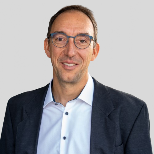
Stefan Kimmerle, Ph.D.
Bosch Sensortec
Dr. Stefan Kimmerle studied physics and economics in Stuttgart, Tübingen and San Diego and graduated with a diploma degree in 2001. Afterwards he continued his studies in physical based modelling and simulations at University Tübingen and INRIA Grenoble and holds a PhD in computer science.
He joined Bosch in 2005 and held various positions in the field of MEMS, semiconductors, customer application and research and development for Automotive sensors. Since 2014 he works in R&D for sensors in consumer electronics, namely smartphones, wearables, and hearables at Bosch Sensortec GmbH. Today he is Vice President Engineering with R&D teams in Germany, Italy, China and USA.
Company Profile
Bosch Sensortec is a wholly owned subsidiary of the Bosch Group, dedicated to developing and marketing a comprehensive portfolio of microelectromechanical systems (MEMS)-based sensors and solutions for consumer electronics. Headquartered in Reutlingen, Germany, the company was founded in 2005 and has since become a global leader in MEMS sensor innovation. Bosch Sensortec’s product offerings include motion sensors, environmental sensors, smart sensors, and software solutions that power a wide range of devices such as smartphones, wearables, drones, and IoT applications.
By leveraging Bosch’s decades of experience and leadership in automotive MEMS sensor technology, Bosch Sensortec brings industrial-grade performance to the consumer market. With a focus on miniaturization, energy efficiency, and intelligent sensing, the company enables smart, connected devices that respond to their environments with precision and reliability. Through continuous innovation and a strong global network, Bosch Sensortec plays a pivotal role in advancing next-generation sensor technologies for an increasingly digital and mobile world.

09:40 – 10:00
Keynote
Wired for Intelligence: SWI3S—The New Interface Standard for Ambient AI
As voice becomes the natural interface for AI systems, especially in wearables and edge devices, the limitations of legacy audio protocols like PDM are increasingly exposed. These older standards lack the scalability, synchronization, and embedded control required for intelligent, multi-microphone architectures.
Enter SoundWire-I3S (SWI3S)—the next-generation interface standard designed to meet the demands of ambient AI. With support for up to 12 peripherals on a single 2-wire bus, dynamic scheduling, and integrated control signaling, SWI3S enables compact, power-efficient microphone arrays that are purpose-built for voice-first interaction.
This talk will explore how SWI3S is already unlocking new possibilities in smart glasses, where products like Meta Ray-Ban and Oakley frames integrate 5+ microphones per unit. These wearables represent a shift toward seamless, conversational AI—where synchronized audio capture and reduced wiring complexity are no longer optional, but foundational.
By aligning MEMS innovation with the rise of ambient intelligence, SWI3S is not just a technical upgrade—it’s the new interface standard for AI communication.

Gunar Lorenz, Ph.D.
Infineon Technologies AG
Dr. Gunar Lorenz is heading the technical marketing and application engineering for consumer sensors at Infineon Technologies. Gunar joined Infineon in 2016 as system project manager responsible for Infineon’s first open market MEMS microphone. Prior joining to Infineon he worked as director of system-level simulation at Coventor, where he and his group invented and developed Coventor’s MEMS/IC co-simulation design environment MEMS+. The original ideas for MEMS+ are embodied in his PhD carried out at Robert Bosch R&D Center in 1999. Gunar graduated in mechanical engineering at the TU Braunschweig in Germany and received his PHD in electrical engineering from the TU Bremen in 1999.
Company Profile
Here at Infineon, we combine entrepreneurial success with responsible action to make life easier, safer, and greener. Barely visible, semiconductors have become an indispensable part of everyday life. We play a key role in shaping a better future – with microelectronics that link the real and the digital world. Our semiconductors enable efficient energy management, smart mobility, as well as secure, seamless communications in an increasingly connected world. Infineon designs, develops, manufactures and markets a broad range of semiconductors and system solutions. The focus of its activities is on automotive and industrial electronics, communication and information technologies, IoT, sensor technology and security. The product range comprises standard components, software, customer-specific solutions for devices and systems, as well as specific components for digital, analog, and mixed-signal applications.

10:05 – 11:05
Networking Break
11:10 – 11:30
MEMS Infinity supports device commercialization in AI Era
MEMS Infinity, Sumitomo Precision Products has an alliance with A.M.Fitzgerald to provide an integrated product development support of PZT MEMS to customers in various markets, and AI is certainly one of them. We can shorten the time to market and reduce the cost of development. MEMS can play an important role in AI Era, not only in edge AI but also in cloud-based AI. Some examples for the different AI applications will be presented to stimulate the audience to have various new ideas for the future.
Hiroshi Miyajima, Ph.D.
MEMS Infinity / Sumitomo Precision Products
Hiroshi Miyajima received the M.S. and Ph.D. degrees in precision machinery engineering from the University of Tokyo, Tokyo, Japan in 1987 and 2004, respectively.
He has been with Sumitomo Precision Products Co., Ltd. since 2021 and is currently a Fellow, ICT Division. He was with Goertek Technology Japan Co.,Ltd. in 2018-2021 and with Olympus Corporation in 1987-2018. He was a visiting research scholar at Case Western Reserve University, USA, in 1992-1994.
Company Profile
MEMS Infinity, Sumitomo Precision Products Co., Ltd., provides seamless foundry services from design to mass production. With expertise in diverse MEMS device development, mass production, and manufacturing equipment, enabling efficient project execution and accelerating commercialization for our clients. Our key strengths lie in high-performance PZT thin-film and Si DRIE technology.
11:35 – 11:55
High Performance MEMS Inertial Sensors Enabling Advanced Mobility
Many applications in mobility and industrial machinery require reliable, robust inertial measurement units (IMUs) that maintain low noise and high accuracy in harsh environments. Precision, safety, and robustness are especially critical in autonomous driving and advanced mobility systems. This talk will provide insight into Murata’s unique MEMS technology and innovative 3-axis sensor concepts behind our new High Performance 6 Degrees of Freedom (6 DOF) Sensor product, demonstrating how it meets these demanding requirements across diverse markets.
Senni Laaksonen
Murata Manufacturing Co., Ltd.
Senni Laaksonen has over 20 years experience of providing inertial sensors to the automotive industry. She started her career at VTI, a company which has been the market leader in low-g accelerometers and Combo sensors for safety critical applications since early 1990s. Murata acquired VTI in 2012. She has been working in various positions in Murata from product design to process development and project management and is currently responsible of the Research and Development activities of Murata Finland. Senni and her development teams work closely especially with automotive industry to provide new innovative inertial sensors for the customers. Future development in Murata is focusing to provide cutting edge products especially to the ADAS and autonomous driving applications.
Senni holds a MSc degree in Electronics manufacturing Technology from Helsinki University of Technology.
Company Profile
Murata Manufacturing Co., Ltd. is a worldwide leader in the design, manufacture and sale of ceramic-based passive electronic components & solutions, communication modules and power supply modules. Murata is committed to the development of advanced electronic materials and leading edge, multi-functional, high-density modules. The company has employees and manufacturing facilities throughout the world. For more information, visit Murata’s website at www.murata.com.
www.murata.com/en-global
Company Products & Services
Research, Production and Sales of Electronic Devices made from fine ceramics

12:00 – 12:20
Do AI Factories Dream of MEMS Sheep?
From the dystopian nanobots dreaded by the cyberpunk authors of 70s to the trillion-sensor networks dreamed by the market analysts of the 2010s, the miniaturization potential afforded by the electronics industry to the sensor world has sparked imaginations. With AI impacting the world around us, where do sensors fit, and where will the next growth come from? Due to physical limitations, the trend will be increasing component functionality and intelligence rather than further reducing footprint. Amkor has a strong presence worldwide and continuously invests, to always be ready to support the next industry expansion!
Nick Renaud-Bezot
Amkor Technology, Inc.
Nick joined Amkor in 2022 and currently serves as Senior Manager, MEMS and Sensors BU. Prior to joining Amkor, he held various business development and engineering positions at USound GmbH, AT&S AG, and SERMA Technologies. Nick holds an MSc degree in Microtechnics from SUPMICROTECH-ENSMM and a Specialized Master’s in Technology and Innovation Management from Grenoble School of Management.
Company Profile
Amkor Technology, Inc. is the world’s largest US headquartered OSAT (outsourced semiconductor assembly and test). Since its founding in 1968, Amkor has pioneered the outsourcing of IC packaging and test services and is a strategic manufacturing partner for the world’s leading semiconductor companies, foundries, and electronics OEMs. Amkor provides turnkey services for the communication, automotive and industrial, computing, and consumer industries, including but not limited to smartphones, electric vehicles, data centers, artificial intelligence and wearables. Amkor’s operational base includes production facilities, product development centers and sales and support offices located in key electronics manufacturing regions in Asia, Europe and the United States. Learn more at https://amkor.com
12:25 – 12:45
Micro Machines, Macro Impact: Powering Societal Change with European MEMS
At the MEMS & Sensors World Summit in Dresden, Kees Wesdorp will present how MEMS and photonics technologies are essential in solving major global challenges—from driving access to healthcare to reducing AI energy consumption. Representing XIVER, he will highlight the company’s evolution from its Philips legacy into a nimble, high-impact European foundry serving global markets. The talk includes real-world examples in healthcare, AR/VR, and photonic integration, emphasizing Europe’s strategic opportunity and XIVER’s ecosystem role. With a call to accelerate lab-to-fab pathways, the presentation frames MEMS not just as tiny components—but as miniature engines of massive, planetary-scale change.
Kees Wesdorp, Ph.D.
XIVER Mems Foundry
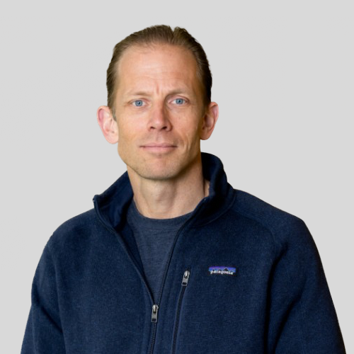
Kees Wesdorp is CEO of DeepHealth, where he leads the development of AI-driven diagnostic platforms transforming radiology and digital health. He also chairs the board at Xiver, Europe’s leading independent MEMS foundry, enabling next-generation technologies for healthtech, photonics, automotive, and industrial applications. Earlier in his career, Kees played a key role in the transformation of NXP Semiconductors, driving global operations and product innovation. He later held executive roles at Philips, leading its Precision Diagnosis division, and at Hellman & Friedman, supporting portfolio value creation. Kees holds a PhD in experimental atomic physics from Vrije Universiteit Amsterdam.
Company Profile
XIVER – More than a MEMS Foundry, leveraging a legacy of innovation
XIVER is a leading independent MEMS foundry specialized in process development, industrialization, and manufacturing of thin-film and MEMS devices.
Empowered by a team of over 110 highly skilled professionals, XIVER leverages decades of innovation and expertise from its Philips heritage.
Utilizing proven process technologies and key-enabling IP-backed platforms, XIVER delivers tailored solutions to its customers active in various markets and applications, including Industrial, Medical, Photonics, and Automotive.
With commitment to excellence, XIVER enables seamless transitions from development to medium-volume production on 200mm wafers, operating in a 2,650m2 cleanroom.
Located at the High Tech Campus Eindhoven, the Netherlands, XIVER is the only independent, pure-play MEMS foundry in Europe, serving customers globally.
Company Products & Services
XIVER offers innovative product platform solutions, such as its cutting-edge CMUT ultrasound platform that powers the next generation of interventional, portable point-of-care, and wearable ultrasound imaging devices. Our streamlined process ensures innovative, high-performance MEMS solutions tailored to your needs.
We employ a phase-gated approach to ensure a predictable and reliable path for MEMS processes, from concept to manufacturing.

12:50 – 13:50
Buffet Lunch
13:55 – 14:15
From Sensing to Thinking: The Evolution of MEMS with Embedded AI
2024 was a welcome turning point for the MEMS industry, with global revenue estimated at $15.4 billion. This is primarily due to the winding down of the inventory stockpiling in the second quarter of 2024. The race for innovation is crucial to maintaining a high sensor value and stabilizing the average selling price (ASP). Implementing first-stage data processing at the sensor level is one possible solution that brings several advantages, from power consumption to versatile applications and ease of integration.
The presentation will provide an overview of the current status of the MEMS industry, key trends expected over the next five years, and insights into the evolution of the MEMS ecosystem within the global economic context.
Pierre-Marie Visse
Yole Group
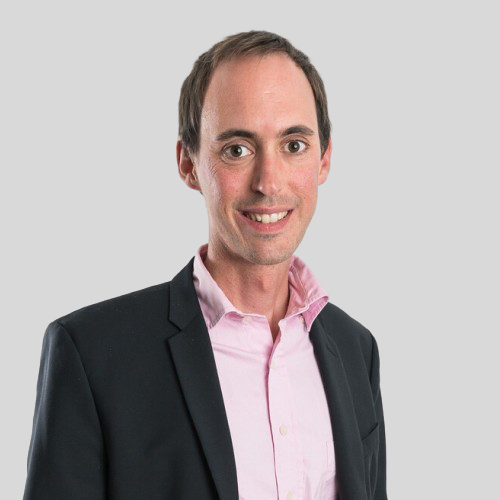
Pierre-Marie Visse is Senior Technology & Market Analyst, MEMS & Sensing at Yole Group. He is working within the Photonics & Sensing team. Pierre-Marie contributes daily to the technical, marketing, and strategic analysis on various MEMS and sensing technologies.Prior to Yole Group, Pierre-Marie served as an R&D project manager at eLichens, specializing in the detection of environmental gases, for more than 2 years. His primary focus was the development of gas sensors and IoT for gas detection. Previously, Pierre-Marie worked at TDK-Tronics for more than ten years as an inertial MEMS designer for custom sensors, accelerometers, and gyroscopes. He then worked as an R&D project manager for the navigation, industrial, and watchmaking industries. Pierre-Marie graduated from ESIEE-Engineering (France) in 2010, specializing in microsystems.
Company Profile
Yole Group is a leading international market research and strategy consulting firm, delivering in-depth analyses across market trends, technology developments, teardowns, and reverse costing. Leveraging deep semiconductor expertise, its team of analysts also provides custom consulting services, offering strategic, technical, and market insights tailored to address specific business challenges and opportunities.

14:20 – 14:40
Beyond the Sensor: How Driver ASICs Unlock Next-Gen MEMS Performance in HMI Applications
Sensors are the cornerstone of modern HMI interfaces—from touch controls to gesture recognition. Yet their full potential hinges on a critical, often overlooked component: high-performance driver ASICs. In this session, GlobalFoundries explores how advanced analog/mixed-signal and BCD process technologies solve key MEMS challenges: signal integrity, power efficiency, system integration, and reliability. Discover how optimized ASIC-MEMS co-design enables smaller form factors, lower latency, and enhanced functionality in automotive, industrial, and consumer HMI systems. We’ll showcase real-world applications and outline a collaborative framework for MEMS designers to leverage GF’s silicon leadership—proving that the right interface is just as vital as the sensor itself.
Ruby Yan, Ph.D.
GlobalFoundries
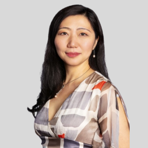
Ruby Yan is a seasoned Business Line Director at GlobalFoundries, where she oversees the Sensing & Display, ID & Security business lines. With over a decade of experience in the company, she has held various roles and responsibilities including technology development and product management. Ruby is not only a Master Inventor with more than 20 patents and over 70 peer-reviewed publications to her name but also a fervent advocate for diversity and inclusion in the tech world. She earned her Ph.D. in Microelectronic Engineering from the National University of Ireland, Cork, and an EMBA from ESCP Business School.
Company Profile
GF is one of the world’s leading semiconductor manufacturers and the only one with a truly global footprint. We are redefining innovation and semiconductor manufacturing by developing feature-rich process technology solutions that provide leadership performance in pervasive high growth markets. As a steadfast partner, with a unique mix of design, development and fabrication services, GF works collaboratively alongside our customers to bring a broad range of innovative products to market. With a global customer base, a talented and diverse workforce and an at-scale manufacturing footprint spanning three continents, GF is delivering a new era of more.

14:45 – 15:05
Microchannel particle deposition for MEMS & Sensors Applications
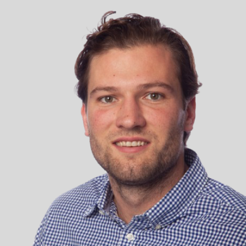
Thomas Russell
Mesoline B.V.
Thomas Russell is the CEO and co-founder of Mesoline. After earning a bachelor’s in physics from the Technical University of Delft in the Netherlands, Thomas moved to Los Angeles to complete his master’s degree at the California Institute of Technology (Caltech), where he studied the application of microchannel particle deposition (MPD) technology under prof. Harry Atwater.
In 2017 he spun-out Mesoline from this research, which led to him being recognized as a Forbes 30 under 30 entrepreneur in 2019. In the same year, after relocating to the Netherlands to expand Mesoline, Thomas raised a $2.5M Horizon 2020 grant from the European Commission and several $M from private investors, which enabled him to further accelerate the development of the MPD technology to a reliable process.
Currently, he’s working on ensuring further growth of the company, market entry of Mesoline with the MPD technology and overseeing the buildup of a new production facility in Rotterdam, The Netherlands.
Company Profile
Mesoline has developed and is scaling up a fundamentally new micro-fabrication process, micro-channel particle deposition (MPD), used to deposit nanomaterials. This wafer-scale thick-film deposition process is a cost-effective and scalable platform technology that enables next generation semiconductor devices such as MEMS & Sensors and other ultra-miniaturized products.
Founded in 2017, Mesoline is headquartered in the Netherlands and enjoys strong financials. Mesoline provides MPD as a contract manufacturing service to semiconductor companies.

15:10 – 15:40
Networking Break
15:45 – 15:55
Coping with complexity – a flexible test system for a wide range of digital sensors
As MEMS sensor technologies evolve and MEMS sensor applications increase in complexity to offer more and more functions also sensor interfaces have become a constantly changing target. To be able to cope with the already existing variety of sensor interface parameters as well as be ready for future advancements in sensor protocols and data rates IDM’s and test service providers need to make smart decisions towards proper test equipment. In this presentation a flexible and cost efficient solution for testing digital sensors will be presented.
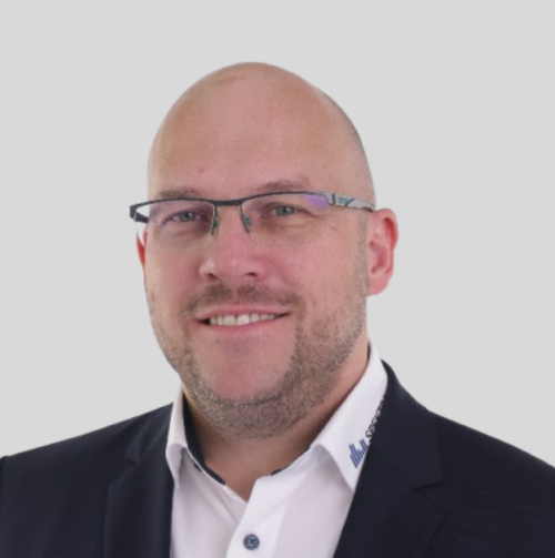
Ingolf Leidert
SPEKTRA GmbH Dresden
Ingolf Leidert is Product Manager Device Testing at SPEKTRA GmbH Dresden, with prior Product Marketing and Application Engineering positions at Atmel Corporation and Advanced Micro Devices. He holds a bachelor’s degree in communications engineering and has over 20 years’ experience in the semiconductor industry. Throughout his career he has worked on various wired and wireless sensor applications and knows the supplier and the customer perspective. At SPEKTRA he is working on efficient sensor testing solutions that help improve MEMS sensor reliability and robustness.
Company Profile
SPEKTRA Schwingungstechnik und Akustik GmbH Dresden, Germany was founded in 1994 and has established itself as a renowned manufacturer of components and systems for the testing and calibration of sensors. The products of the family business are used worldwide for the reliable measurement of dynamic physical quantities such as vibration, acceleration, sound pressure or alternating charge.
As from 2008, SPEKTRA also includes the APS trademark under which the company manufactures and sells long-stroke vibration exciters (shakers) and runs a marketing office in California, USA under the name of APS Dynamics, Inc. Through this merger, forces based on decades of experience could be bundled to develop a new generation of even more powerful vibration control systems.
Furthermore the company‘s calibration laboratory is accredited by DAkkS and offers a wide range of calibration services. And all this at a level of measurement uncertainty that can normally only be guaranteed by topmost national metrology laboratories.
SPEKTRA is often pioneer when it comes to the development, manufacturing or distribution of measuring and testing systems as well as calibration equipment. The use of such technology to provide special services and equipment for metrological and industrial applications enabled the company to reach an international top position in a growing market.
SPEKTRA LABS is your brand for excellence. With an international network of laboratories in Europe and the USA, we offer a wide range of testing and calibration services for dynamic measurement parameters – including vibration, shock, sound level as well as tilt and rotation rate.
Our accredited laboratories combine state-of-the-art technology with certified processes: So that you can rely on correct measuring results and smooth processes at all times.
Company Products & Services
MEMS-Testing at different levels (Lab and Fab):
From individual laboratory-scale sensor technology to highfrequency mass production. TESTelligence for MEMS sensors. Discover our S-TEST systems.
S-TEST Lab:
The S-TEST Lab systems offer a wide range of sensor system tests for development and laboratory environments. Its flexible system components allow users to quickly respond to different test requirements and sensor types. From parametric tests, functional tests, measurement comparisons, to characterization, our system solutions provide sensor developers with comprehensive capabilities for early detection of design flaws.
S-TEST Fab – optimized functions for efficient mass testing
The S-TEST 16 Fab systems are designed for use in the mass production of sensors. Their optimized design allows operation in temperature controlled cabinets. Variable throughput rates and test coverage can be achieved from small test series to highly parallel testing of several hundred sensors.
Calibration system CS Q-LEAP:
Sensor calibration is our core competence. Calibration laboratory SPEKTRA
The product group “Calibration Solutions” includes calibration systems as well as services. The SPEKTRA family of CS18 and the newest CS Q-LEAPTM calibration systems offers the calibration for the following measurands:
Acceleration (0.05 Hz … 350 kHz)
Shock (few mm/s² … 2,000 km/s²)
Acoustics (0.1 Hz … 20 kHz, until 124 dB)
Dynamic Force (10 Hz … 1 kHz, few mN … 20 kN)
Dynamic Pressure (up to 4,000 bar)
Mobile calibration system CV-10:
The CV-10 provides all the benefits of a mobile system. With the proven user-friendly interface of SPEKTRA.
Discover how smart, easy and flexible the on-site test and calibration of accelerometers, proximity probes and velocity sensors can be.

16:00 – 16:10
Demands for sensor test from development to high-volume manufacturing
Basic needs for MEMS and sensor test and calibration systems remains the same from product development to manufacturing, there’s significant differences on detail level. Presentation describes Pentamaster approach of transferring from laboratory system to mid- and high-volume production using the example of a ambient light sensor (ALS).
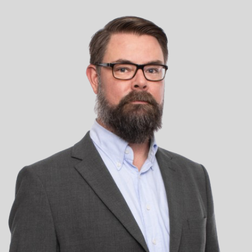
Ari Kuukkala
Pentamaster Technology Sdn. Bhd.
Ari has near 20 years of experience in MEMS sensor assembly automation and test by several roles over the years. His career started as mechanical design engineer for sensor test equipment, and later continued field service and research & development as well as Sales Director, GM and BU Director positions. In the current position of Development Manager in Pentamaster, he is responsible to architect and bring to market new test solutions in the area of semiconductor test, focusing still in MEMS.
Company Profile
Pentamaster Group provides automation technology and solutions to multinational manufacturers in the automotive, semiconductor, electro-optical, consumer electronics, and medical sector, spanning across APAC, North America and Europe. Besides the HQ and production plant in Penang, Malaysia, the Group has strategic presence globally with offices located in the USA, Japan, Germany, Singapore and production facilities in China.
With the speed and magnitude of technology progress today, Pentamaster Group will always be bold enough to explore new innovations. For years, the Group has been one of the leading global providers of automated test equipment to suit different requirements and needs of customers from various industries. In the automotive segment, the group has developed a proprietary SiC wafer burn-in system, being one of the top four manufacturers in the world, in creating a niche market space for this growth sub-segment and to solidify the Group’s position in the automotive industry.

16:15 – 16:25
Navigating the Complexities of Wafer Level Chip Scale Package (WLCSP) MEMS Testing
The rapid adoption of Wafer Level Chip Scale Package (WLCSP) technology is revolutionizing MEMS manufacturing, enabling unprecedented miniaturization, higher integration, and cost efficiencies critical for the next generation of smart devices, automotive systems, and IoT applications. However, this advancement introduces significant challenges in device testing, particularly concerning precision handling, accurate probing, and addressing device-specific environmental sensitivities.
This presentation will delve into the critical hurdles faced in WLCSP MEMS testing, emphasizing solutions that ensure quality and reliability in high-volume production. We will explore the imperative for ultra-accurate pick-and-place mechanisms that prevent ‘stuck devices’ and safeguard delicate surfaces, alongside advanced probing techniques for fine-pitch contacts. Furthermore, the session will highlight specialized test considerations for challenging device families: from the necessity of isolated test environments for inertial sensors to mitigate acoustic and mechanical noise, to stringent contamination control measures for imaging sensors that demand pristine surfaces. The discussion will also cover the advantages of integrated test processes, where a single machine handles devices from diced wafer to tape and reel, significantly boosting efficiency and minimizing the risk of damage due to handling processes. Finally, we’ll touch upon the role of auto-maintenance functions in enhancing handler reliability and optimizing preventive maintenance schedules.
Attendees will gain valuable insights into the latest innovations and best practices for overcoming the unique complexities of WLCSP MEMS testing, contributing to robust and cost-effective manufacturing workflows for a rapidly expanding market.
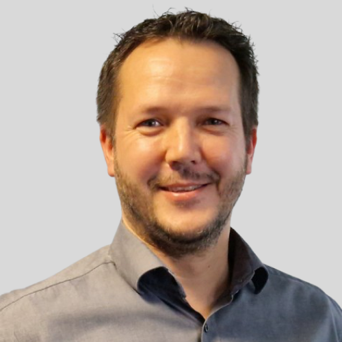
Oleg Fotteler
SPEA S.p.A.
Oleg Fotteler received his degree in Electrical Engineering in 2005. He started developing test solutions for semiconductor products in SPEA Germany throughout his studies. After his graduation, Oleg kept on his career for four years in the same company as an Application Engineer for board testing, when in 2009 switched to the Semiconductor Sales Department. Starting from 2013 up to the present day, he supports SPEA partners in North and East Europe with sales activities related to all SPEA products.
Company Profile
Established in 1976, SPEA is a world leading company in the field of automatic test equipment for ICs, MEMS, sensors, electronic boards. SPEA serves the big semiconductor IDMs and OSATs with the most cost-effective and high-performance equipment to test automotive, SoCs, analog mixed-signal devices, MEMS sensors and actuators, power and discretes, identification devices, delivering highest measurement capabilities, lowest cost of test and fastest time-to-market. SPEA systems are designed to detect any possible defect in electronic products, so that they won’t fail on the field. High throughput, best detection capability, test techniques designed on the latest technologies requirements, complete configurability. For SPEA customers, testing is not an additional cost, but a tangible competitive advantage.
Company Products & Services

16:30 – 16:40
Faster MEMS Development: Reducing Tapeouts
MEMS development is time-consuming and costly. As mechanical structures—whether accelerometers, gyros, or micromirrors—become more complex, meeting specifications grows increasingly difficult. Process Design Kits (PDKs) are also more sophisticated, adding to the challenge. This presentation demonstrates how to significantly reduce the number of tapeouts needed to develop a production-ready sensor. Learn how advanced modeling and simulation can accelerate development, cut costs, and improve first-time-right success. Whether you’re designing next-generation inertial sensors or or revise existing designs, this talk provides practical methods to streamline your design process and shorten time-to-market.
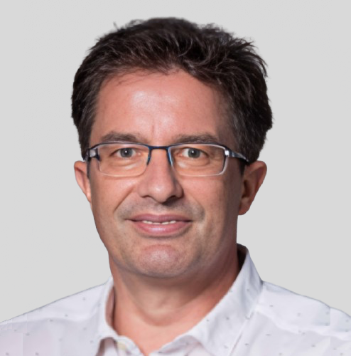
Jan Mehner
i-ROM
Jan Mehner has been working in the field of design and simulation for MEMS for over 30 years. He spent many years as a MEMS consultant for NXP, Bosch, and other companies. Since 2007, he has been teaching Microsystems at the Technical University of Chemnitz in Germany. In 2015, he founded i-ROM, which develops simulation software specifically for the design of MEMS and provides consulting services.
Company Profile
We are a MEMS design house offering both MEMS design consulting and software specifically for MEMS design, the i-ROM MODELBUILDER.
If you have an idea for a MEMS sensor – we have the way to get there. Whether it’s micromirrors, angular rate sensors or gyroscopes. We help you with the design until your MEMS sensor meets the desired requirements. Our software covers the entire design process, from the idea for a sensor to the complete manufacturing-ready GDS interface. All process data kits (PDK) are also taken into account right from the beginning.
With our software you can shorten the expensive and lengthy design process from an average of 3 to up to 1.5 years. Time that is worth a tremendous amount of money.
i-ROM MODELBUILDER is the new generation of simulation software. It is suitable for both experienced engineers and beginners. Its graphical user interface and intuitive operation make it a must for every MEMS company. The i-ROM software toolbox has its own FEM core, electronics and GDS interfaces. Easy to use – easy to start.
Company Products & Services
MEMS Consulting Services and MEMS simulation software
16:45 – 16:55
Public funding opportunities for the semiconductors industry in the EU
The semiconductors industry is among the highest beneficiaries of public funding in the EU. Grants target R&D activities, first industrial deployment of breakthrough innovations and first of a kind manufacturing facilities. Securing such State aid and EU funding is a highly competitive process which requires a thorough understanding of the numerous opportunities and associated regulations. Based on several use cases, Marc Isabelle’s presentation will provide a valuable first dive into public funding opportunities for the semiconductors industry in the EU.
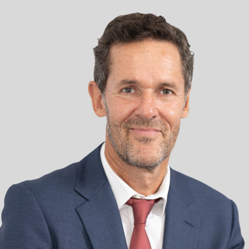
Marc Isabelle, Ph.D.
european economics
Marc ISABELLE, engineer & PhD in Economics, is the founder and CEO of european economics.
Marc is a recognised expert in the public funding of strategic projects. Since 2009, he has helped 195 companies secure €41 billion in public funding for 246 major projects. These initiatives tackle key societal challenges – including disruptive innovation, decarbonisation, resilience and infrastructure – across a wide range of industrial sectors including microelectronics, software, telecoms, automotive, energy and environment, batteries, pharmaceuticals and biotech.
Through his extensive work with the European Commission and national authorities, Marc has actively contributed to shaping the methodologies and best practices used to assess public funding applications and their compatibility with EU regulations.
Company Profile
Founded in 2009, european economics is a recognised pure-player consultancy specialising in public funding. We deliver tailored, high value-added services across Europe to support our clients in designing and implementing turnkey public funding strategies – State aid and European funding – for their most strategic projects:
• €41 billion in public funding secured for 246 projects, including €5.8 billion in 2024,
• 100% success rate for State aid notifications to the European Commission.
Company Products & Services
We support our clients with a turn-key approach at every step of their project’s life-cycle: funding strategy definition, application file preparation (at National and EU level), European Commission validation process, and funding monitoring.
17:00 – 17:45
Panel Session: Breakthrough Innovations, Industry Collaborations and Roadmap
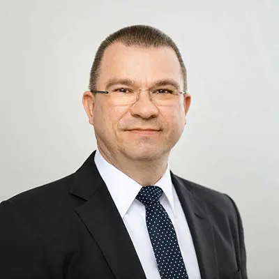
Moderator
Jörg Amelung
Fraunhofer Institute for Photonic Microsystems
Jörg Amelung is Deputy Director of the Fraunhofer Institute for Photonic Microsystems (IPMS) and heads the MEMS Engineering, Manufacturing & Test division. Fraunhofer IPMS is a leading research institute in the MEMS field, equipped with high quality microsystem cleanrooms (200 – 300 mm wafer). As an expert and manager in MEMS technology, Jörg Amelung has been driving the development of smart microsystem technologies since 1993. He also played a key role in OLED development and founded two companies specializing in this field.
Company Profile
Fraunhofer IPMS is a leading international research and development service provider for electronic and photonic microsystems in the application fields of Smart Industrial Solutions, Bio and Health, Mobility as well as Green and Sustainable Microelectronics. Research focuses on customer-specific miniaturized sensors and actuators, MEMS systems, microdisplays and integrated circuits as well as wireless and wired data communication, neuromorphic and quantum computing. Services range from consulting and design to process development and pilot series production.
The Fraunhofer IPMS is one of 75 institutes of the Fraunhofer-Gesellschaft, the leading organization for applied research in Europe. With nearly 32,000 employees Fraunhofer operates with an annual budget of €3.6 billion, €3.1 billion of which is generated by contract research — Fraunhofer’s core business model.
Company Products & Services
The range of services includes wafer processing, characterization & testing, assembly and interconnection technology and the organization of external and supplier services. At the Center Nanoelectronic Technologies (CNT), Fraunhofer IPMS offers applied research, process and material development on 300 mm wafers for microchip producers, suppliers, device manufacturers and R&D partners. 4000 m² of clean room space is available for processing customer orders as well as laboratory space for over 80 processing and analytical tools.


Panelist
Ken Diest
Meta
Ken Diest is a Research Manager and Tech Lead at Meta’s Reality Labs, where he leads programs focused on MEMS and micro-actuator technologies. His focus is on developing these technologies from early stage through production to address critical opto-mechanical and display challenges in AR/MR.
A Materials Scientist by training, Ken’s prior work focused on tunable devices and materials with an emphasis on optical systems. He was the editor and co-author of the book Numerical Methods for Metamaterial Design, and has previously held technology development roles at Apple, MIT Lincoln Laboratories, and Northrop Grumman that focused on new displays and nano-photonics.
Company Profile
Meta builds technologies that help people connect, find communities, and grow businesses. When Facebook launched in 2004, it changed the way people connect. Apps like Messenger, Instagram and WhatsApp further empowered billions around the world. Now, Meta is moving beyond 2D screens toward immersive experiences like augmented and virtual reality to help build the next evolution in social technology.


Panelist
Alastair Attard
UTAC Group
Alastair Attard is Director of Business Development at UTAC Group. He has a Bachelor’s degree in Mechanical Engineering and an Executive MBA, and brings over 19 years of experience in the semiconductor assembly & test.
Alastair has previously held positions at STMicroelectronics in MEMS and SiP process engineering and package development, and at Besi where he managed the process development group for advanced die attach technologies.
Alastair joined UTAC in 2018 and today is responsible for business development of semiconductor assembly and test solutions with particular focus on MEMS, Sensing, and Advanced Packaging.
Company Profile
UTAC Group is a leading outsourced semiconductor assembly and test (OSAT) provider, founded in 1997 and headquartered in Singapore. The company specializes in advanced assembly and test services for logic, memory, analog/mixed-signal, image sensors, MEMS, and power devices. UTAC supports a global customer base that includes fabless companies, integrated device manufacturers (IDMs), and wafer foundries.
With ten manufacturing facilities across Singapore, Thailand, China, and Indonesia, and a robust global sales network spanning North America, Europe, Greater China, Japan, and Southeast Asia, UTAC delivers comprehensive turnkey solutions—from wafer probing to final testing.
UTAC serves diverse market segments including automotive, computing, communications, consumer electronics, and industrial applications. Renowned for its reliability, technological expertise, and customer-centric approach, UTAC continues to play a vital role in enabling next-generation semiconductor innovation.
Company Products & Services
UTAC Group provides a comprehensive range of semiconductor assembly and test services, delivering turnkey solutions from wafer probe to final test across key end markets.
Its packaging portfolio includes leadframe-based packages such as QFN, DFN, QFP, TLA, and Cu-clip variants, as well as laminate-based BGA/iBGA packages for mobile, computing, and automotive applications. UTAC also offers System-in-Package (SiP) modules that integrate multiple components into compact, high-density solutions for IoT, wearables, and automotive electronics.
Advanced wafer-level offerings include bumping services and Wafer-Level Chip Scale Packaging (WLCSP) for customers requiring miniaturization, high electrical performance, and low-profile form factors.
UTAC also supports image sensor packaging, including automotive-grade iBGA with cleanroom assembly to meet stringent reliability and contamination standards.
To complement mass production, UTAC provides value-added services such as package design support, reliability qualification, and failure analysis—helping customers accelerate time to market with confidence.

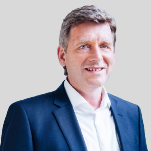
Panelist
Volker Herbig
X-FAB
Volker Herbig, VP BU Microsystems at X-FAB, oversees all MEMS activities within the X-FAB Group. Before assuming his current role, Volker worked as Director Product Marketing at X-FAB. Previously he held also engineering, marketing and management positions at Siemens, Inkjet Technologies and Carl Zeiss where, among other activities, he developed MEMS inkjet print heads and was responsible for setting up a manufacturing facility for those. Volker Herbig holds a master’s degree in physics from Humboldt University, Berlin, Germany.
Company Profile
X-FAB is one of the world’s leading specialty foundry groups for analog/mixed-signal semiconductor technologies with a clear focus on automotive, industrial, and medical applications. As a pure-play foundry, X-FAB provides manufacturing and design support services to customers that design analog/mixed-signal integrated circuits (ICs) and other semiconductor devices for use in their own products or the products of their customers. Its customers worldwide benefit from the highest quality standards, manufacturing excellence and innovative solutions by using X-FAB’s modular CMOS and SOI processes in geometries ranging from 1.0 µm to 110 nm, and its special micro-electro-mechanical systems (MEMS) processes. X-FAB is also the first pure-play foundry to provide comprehensive processing technologies for the wide-bandgap materials silicon carbide (SiC) and gallium nitride (GaN). The GaN-on-Si wafers are manufactured in its modern 8” fab in Dresden, Germany, and SiC wafers in the 6” fab in Lubbock, Texas, USA. X-FAB runs six production facilities in Germany, France, Malaysia and the U.S. The company employs about 4,200 people worldwide.

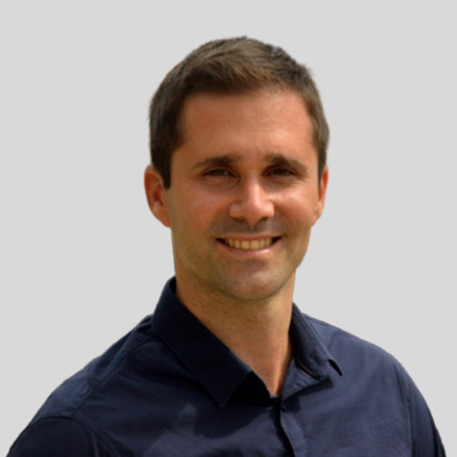
Panelist
STMicroelectronics
Andreja Erbes has been the Director of Technology Scouting and R&D Partnerships at STMicroelectronics since 2022, actively driving innovation initiatives within ST’s Innovation Office. He received the M.Eng., M.A., and Ph.D. degrees from the Department of Engineering, University of Cambridge, in 2011, 2014, and 2015, respectively, specializing in MEMS and mmWave Analog/RF circuit design. He currently serves as Vice President of the IEEE Ultrasonics, Ferroelectrics, and Frequency Control Society (IEEE UFFC).
Company Profile
At ST, we are more than 50,000 creators and makers of semiconductor technologies mastering the semiconductor supply chain with state-of-the-art manufacturing facilities. An integrated device manufacturer, we work with more than 200,000 customers and thousands of partners to design and build products, solutions, and ecosystems that address their challenges and opportunities, and the need to support a more sustainable world. Our technologies enable smarter mobility, more efficient power and energy management, and the wide-scale deployment of cloud-connected autonomous things. We are committed to achieving our goal to become carbon neutral on scope 1 and 2 and partially scope 3 by 2027. Further information can be found at www.st.com.

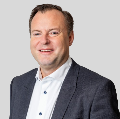
Panelist
Tomas Bauer
Silex Microsystems
With over 20 years at Silex Microsystems, Tomas Bauer has been a driving force behind the company’s global leadership in MEMS innovation. As Executive Vice President of Sales & Business Development, he has played a central role in shaping Silex’s strategic roadmap and fostering long-term collaborations with leading technology innovators. A mechanical engineer by training, Tomas began his career at Ericsson’s wafer fab, where he bridged engineering and commercial roles. Since joining Silex in 2004, his deep industry insight and commitment to breakthrough partnerships have helped position the company at the forefront of next-generation MEMS manufacturing and ecosystem development.
Company Profile
Silex Microsystems AB, a Swedish company, is the world’s leading pure-play MEMS foundry, trusted by the most innovative companies to bring breakthrough ideas to market—faster.
With unmatched expertise and advanced MEMS manufacturing capabilities, Silex turns groundbreaking designs into manufacturable, scalable products, from concept to high-volume production.
Our cutting-edge wafer fab, combined with industry leading process technologies, empowers customers to scale disruptive solutions with confidence, speed, and quality.

18:00 – 21:30
Cocktail Networking Reception & Gala Dinner at Hilton Dresden
Awards Ceremony
End of content
End of content