2-3 December 2025
Tokyo
17:00 – 17:10
State-of-the art solutions for AI Chip manufacturing
Over the past nine months, the AI chip boom has accelerated considerably. High-bandwidth memory (HBM) chips, which are an essential part of AI chips, are undergoing rapid technological advancements. While temporary bonding will still be needed for wafer thinning of HBM3 chips and following generations, production of HBM chips is supposed to shift from thermal compression (TC) bonding to hybrid bonding solutions. TC may still be the preferred option for HBM4, as hybrid bonding is significantly more expensive. However, with HBM5 at the latest, the switch to hybrid bonding is expected to take place due to higher I/O densities. SUSS MicroTec has developed a D2W hybrid bonding solution together with flip-chip bonder specialist SET and also offers W2W hybrid bonding solutions, thus providing the technologies required for the next generations of HBM and AI chips.

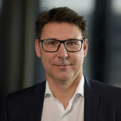
Robert Wanninger
SUSS
Robert Wanninger is Senior Vice President of the Advanced Backend Solutions (ABS) business unit at SUSS. With leading equipment and process solutions for Imaging, Coating and Bonding applications, SUSS ABS business unit is well positioned to serve the semiconductor industry. Robert brings ~25 years of experience in semiconductor industry. Prior to joining SUSS in 2021, he has worked over 20 years at Infineon in various management positions and spend two years in Korea as COO of LS Power Semitech. He holds a PhD in Chemistry from the University of Regensburg, Germany.
SUSS
Company Profile
SUSS is a leading supplier of equipment and process solutions for microstructuring in the semiconductor industry and related markets. In close cooperation with research institutes and industry partners SUSS contributes to the advancement of next-generation technologies such as 3D Integration and nanoimprint lithography as well as key processes for MEMS and LED manufacturing. With a global infrastructure for applications and service SUSS supports more than 8,000 installed systems worldwide. SUSS is headquartered in Garching near Munich, Germany. For more information, please visit suss.com.
Company Products & Services
The SUSS portfolio covers a comprehensive range of products and solutions for backend lithography, wafer bonding and photomask processing, complemented by micro-optical components. After sales, the company supports the entire life cycle of the tools: its range of services begins with the installation and startup of the systems including user training. Once systems are integrated in the customer’s environment, SUSS provides consistent support. Since long life cycles are very common for the company’s equipment, preventive maintenance programs are available, as well as reliable spare parts systems, warranty extensions and system upgrades. SUSS maintains service locations and local support teams in all areas of the globe to provide quick help.
