


Redefining Semiconductor Excellence: Innovation, Sustainability, and Global Transformation
Theme: Automotive Electronics Technology Innovation and Development
主题:汽车电子技术创新与发展
07:30 – 08:50
Registration 签到注册
09:00 – 09:10
Welcome Speech

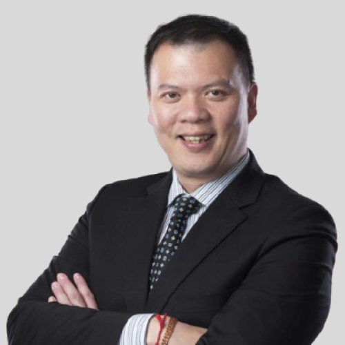
Shaojun Wei
Professor
Tsinghua University
魏少军,应用科学博士,清华大学教授,国际电气和电子工程师协会会士(IEEE Fellow),中国电子学会会士(CIE Fellow),亚太人工智能学会会士(AAIA Fellow),国际欧亚科学院院士,俄罗斯工程院外籍院士;国家集成电路产业发展咨询委员会委员;中国半导体行业协会副理事长,世界半导体理事会中国 JSTC 主席,长期致力于超大规模集成电路设计方法学研究、可重构计算架构研究和通信专用集成电路技术研究,主要研究领域为:超大规模集成电路设计方法学研究,高层次综合技术研究,嵌入式系统设计技术研究和可重构计算技术研究。发表学术论文近300 篇,出版专著 10 册,曾获国家技术发明二等奖、国家科技进步二等奖及多项省部级科学技术奖等。
Wei Shaojun, Doctor in Applied Science, Professor of Tsinghua University, IEEE fellow, CIE Fellow, AAIA Fellow, academician of the International Eurasian Academy of Sciences, Foreign Academician of the Russian Academy of Engineering, Member of the National Integrated Circuit Industry Development Advisory Committee, Vice Chairman of China Semiconductor Industry Association and Chairman of World Semiconductor Council China JSTC, has long been committed to the research on VLSI design methodology, reconfigurable computing architecture and Communication ASIC technology. His main research fields are: Research on IC design methodology and high-level synthesis technology, embedded system design technology and reconfigurable computing technology. He has published nearly 300 academic papers and 10 monographs, has won the second prize of national technological invention, the second prize of national scientific and technological progress and a number of provincial and ministerial science and technology awards.
Company Profile
The campus of Tsinghua University is situated in northwest Beijing on the site of the former imperial gardens of the Qing Dynasty, and surrounded by a number of historical sites.
Tsinghua University was established in 1911, originally under the name “Tsinghua Xuetang”. The school was renamed “Tsinghua School” in 1912. The university section was founded in 1925. The name “National Tsinghua University” was adopted in 1928.
The faculty greatly valued the interaction between Chinese and Western cultures, the sciences and humanities, the ancient and modern. Tsinghua scholars Wang Guowei, Liang Qichao, Chen Yinque and Zhao Yuanren, renowned as the “Four Tutors” in the Institute of Chinese Classics, advocated this belief and had a profound impact on Tsinghua’s later development.
Tsinghua University was forced to move to Kunming and join with Peking University and Nankai University to form the Southwest Associated University due to the Resistance War against the Japanese Invasion in 1937. In 1946 The University was moved back to its original location in Beijing after the war.
After the founding of the People’s Republic of China, the University was molded into a polytechnic institute focusing on engineering in the nationwide restructuring of universities and colleges undertaken in 1952. In November 1952, Mr. Jiang Nanxiang became the President of the University. He made significant contributions in leading Tsinghua to become the national center for training engineers and scientists with both professional proficiency and personal integrity.
Since China opened up to the world in 1978, Tsinghua University has developed at a breathtaking pace into a comprehensive research university. At present, the university has 20 schools and 59 departments with faculties in science, engineering, humanities, law, medicine, history, philosophy, economics, management, education and art.
With the motto of “Self-Discipline and Social Commitment” and the spirit of “Actions Speak Louder than Words”, Tsinghua University is dedicated to the well-being of Chinese society and to world development. As one of China’s most prestigious and influential universities, Tsinghua is committed to cultivating global citizens who will thrive in today’s world and become tomorrow’s leaders. Through the pursuit of education and research at the highest level of excellence, Tsinghua is developing innovative solutions that will help solve pressing problems in China and the world.
魏少军教授致欢迎词
09:10 – 09:25
Welcome and Product speech

Gerald Yin, Ph.D.
Chairman and CEO
AMEC
Dr. Gerald Yin has served as AMEC’s chairman and CEO since the company was founded in 2004. He is the chief founder of AMEC and one of major leaders for worldwide plasma etch technology, product development and commercialization.
He worked in Silicon Valley for 20 years with Intel Central TD as a senior process engineer, Lam Research as Etch R&D department manager, and then worked for Applied Materials at different executive positions including CTO and later General Manager of Etch Product Business Group, and Corporate Vice President. He participated in and led a number of the most successful CCP and ICP plasma etcher development which help Lam Research and Applied Materials gaining etch market leader position. He is the major inventor of 90+ US patents and 200 other country patents.
Gerald have pursued chemical reactor development for more than 60 years with nearly 40 years’ experience in plasma etch ,thin film technology and equipment development. Dr. Yin graduated from Beijing Fourth High School and received BS from University of Science and Technology China in year 1967, after 10 years working for Petrochemical industry and Chinese Academy of Sciences, he pursued graduate study in Physical Chemistry at Beijing University .He went to US in 1980 and received Ph.D. in Physical Chemistry from University of California (UCLA).
Draying was awarded the Outstanding Contribution Award for National Science and Technology Major Projects in 2010, received Magnolia Award of Shanghai in 2012. He was listed one of “Top Ten Pudong Economic Figures” in 2013, listed as one of “ 11 Figures of the Year in Shanghai“ in 2018. Together with Intel Chairman and other distinguished semi executives, Dr. Yin was named one of Top 10 “All Stars of International Semiconductor Industry” in 2018 by VLSI Research.
In 2020, Dr. Yin was named “ 50 Best CEOs in China “by Forbes. He was named as the sole major winner of 2021 Ernest Young Entrepreneur in China. He ranked 1st among the top ten “Best leaders of China Public Companies” by Security News in 2022 .He was named “ 50 Best CEOs in China” again by Forbes in 2025 and featured on the front cover of the Forbes Magazine in 2025 July.
尹志尧博士是中微公司首席创始人,21 年来一直担任董事长兼首席执行官。他参与尹志尧博士是中微公司首席创始人,21 年来一直担任董事长兼首席执行官。他参与并领导了国际集成电路设备业界一半以上成功的等离子体刻蚀设备开发,是几代等离子体刻蚀技术及设备的主要发明人和工业化应用的推动者之一。
尹博士曾在美国硅谷先后担任英特尔公司中心研发部资深工程师(Intel)、半导体设备的龙头公司—泛林公司(Lam Research)刻蚀机研发部主管和应用材料公司(Applied Materials)等离子体刻蚀事业群总经理及总公司副总裁。帮助上述企业成为国际等离子体刻蚀设备领先的公司。他也是 90多项 项美国专利和 200多项其他国家专利的主要发明人。
尹志尧博士从事物理化学反应器技术 62年。1967 年获中国科技大学化学物理学士学位,曾在石化部兰州炼油厂及中科院兰州化物所工作。1978年进入北京大学化学系就读研究生,1980 年赴美留学,于 1984 年获得了美国加州大学洛杉矶分校(UCLA)物理化学博士学位。
尹志尧博士在 2010 年获得国家科技重大专项突出贡献奖,2012 年获得
上海市“白玉兰纪念奖”,2013 年获得首届“浦东经济人物十强”,2018 年获得
“感动上海年度人物”11 人之一。2018 年获评国际半导体产业十大领军明星(All
Stars)。2020 年和荣登福布斯 50 名中国最佳 CEO 之一。2021年获得安永中国唯一的企业家大奖。2022 年在证券时报中国上市公司价值评选中,获得“中国上市公司年度领军人物奖”,并名列第一。2023 年获得上海市政府评定的“上海市科技进步奖”一等奖。2025年第二次荣登福布斯中国最佳50名CEO之一, 并成为福布斯中国杂志封面人物。
Company Profile
Advanced Micro-Fabrication Equipment Inc. China (AMEC) is one of the most technologically advanced flagship enterprises in China’s integrated circuit (IC) equipment industry. It was among the first batch of companies listed on the STAR Market (Science and Technology Innovation Board) with the stock code: 688012.
Focused on the forefront of global technology, AMEC specializes in the research, development, manufacturing, and sales of critical semiconductor equipment such as plasma etching equipment, deep silicon etching equipment, and MOCVD systems used in the production of integrated circuits, LED chips, and other microdevices.
The company’s plasma etching equipment is widely used in advanced international manufacturing lines for 14nm, 7nm, and 5nm nodes, and it has also made significant progress in nodes below 5nm. AMEC’s MOCVD equipment has achieved a dominant position in both domestic and international markets for blue-light LED production.
In July 2019, AMEC was listed as one of the first 25 high-tech companies on the STAR Market and became the first company on the board to reach a market capitalization of over RMB 100 billion.
As of the end of June 2022, the company had filed 2,089 patent applications, with 1,189 patents granted.
In 2017, AMEC was the only Chinese company mentioned in a major report submitted by the U.S. President’s Council of Advisors on Science and Technology titled “Ensuring Long-Term U.S. Leadership in Semiconductors.”
In the Global Customer Satisfaction Survey for semiconductor equipment conducted by renowned U.S. consulting firm VLSI Research, AMEC ranked third globally in overall satisfaction in both 2018 and 2019. Specifically, it ranked second in plasma etching and first in chemical film equipment, making it the only Chinese chip equipment company to be included in the rankings — highlighting AMEC’s globally competitive and widely recognized products.
中微半导体设备(上海)股份有限公司是国内技术最领先的集成电路设备旗舰企业之一,是科创板首批上市企业(股票代码:688012)。面向世界科技前沿,中微公司聚焦用于集成电路、LED芯片等微观器件领域的等离子体刻蚀设备、深硅刻蚀设备和MOCVD设备等关键设备的研发、生产和销售。公司等离子体刻蚀设备已广泛应用于国际先进的14纳米、7纳米和5纳米生产线。在5纳米以下也取得了很好的进展。公司MOCVD设备在蓝光LED领域已占据国内外市场的主导地位。中微于2019年7月和25家高科技公司在科创板第一批上市,是科创板第一个达到千亿市值的公司。截至2022年6月底,公司申请了2089 项专利,已取得授权1189项。美国科技专家委员会2017年提交美国总统《确保美国在半导体产业的长期领导地位》的长篇报告,报告中唯一提到的中国公司就是中微公司。在美国知名咨询机构VLSI Research举办的全球半导体设备公司“客户满意度”调查和评比中,中微公司2018年及2019年综合评分均为全球第三,等离子体刻蚀名列第二,化学薄膜设备名列第一,也是唯一上榜的国内芯片设备企业,展现公司产品全球领先的竞争力和市场认可度。
欢迎词及产品创新 / 尹志尧博士 / 中微半导体
09:25 – 09:55
I.S.I.G. 15th Year Anniversary Panel Discussion I.S.I.G. 15周年特别企划
Topic: Bridging China and the Middle East: Growth Drivers for Chinese Enterprises in the Gulf Region
连接中国与中东:中国企业在海湾地区的增长动力

Moderator
Salah Nasri
CEO and Co-Founder
International Semiconductor Industry Group (ISIG)
Salah Nasri is the CEO and Co-Founder of the International Semiconductor Industry Group (ISIG), a global organization founded in 2010 that connects and empowers semiconductor decision-makers through strategic leadership platforms, executive summits, and collaborative initiatives. ISIG has become a trusted global hub for industry leaders driving innovation and progress across the semiconductor value chain.
With extensive experience across the semiconductor sector, Salah has played a pivotal role in fostering global collaboration among industry leaders. Under his leadership, ISIG has evolved into one of the most influential communities in the semiconductor ecosystem—bringing together executives, innovators, and policymakers across regions including the United States, Europe, Asia, and the Middle East.
Salah has been instrumental in expanding ISIG’s reach and impact, curating high-level summits and initiatives that drive dialogue and progress across critical areas such as semiconductor manufacturing, AI, MEMS, automotive electronics, and advanced packaging. His vision continues to position ISIG as a key platform for thought leadership, networking, and strategic industry alignment.
Earlier in his career, Salah held positions at Credit Suisse, Goldman Sachs, Worldwide Business Research, and the International Business Development Group. He studied International Relations and Economics at Oxford University and Loughborough University, and in 2024 became a Stanford University alumnus after completing the Stanford Executive Program. In addition to his role at ISIG, Salah also serves on the Advisory Board of Atlant3D, a pioneer in atomic-layer advanced manufacturing solutions.
Company Profile
Established in 2010, the International SemiconductorIndustry (I.S.I.G.) is a prestigious & trusted associationwithin the semiconductor industry, renowned fororchestrating major regional summits across the globe,ranging from the U.S, the Middle East & Asia via ourdivision, the International Semiconductor ExecutiveSummits (I.S.E.S.). Our summits are fully endorsed bylocal governments and leading companies in all areas ofthe semiconductor supply chain.
Moreover, I.S.E.S. serves as the Premier platform for senior executives in technology, manufacturing, and R&D from diverse semiconductor companies, technology providers, and affiliated industries.
Our events are instrumental helping to shed light onto key industry trends, drive innovation and influence key decisions to help shape, and advance the growth of the semiconductor sector.
Panelist
Allan Zhou, Ph.D.
Senior Advisor
SiNan IC Innovation Center Lingang FTZ Shanghai
Allan Zhou holds a Ph.D. in Chemistry and Materials Science from the University of Connecticut, USA.
He has served as CEO of Shanghai GTA Semiconductor Co., Ltd., Professor at Fudan University, Distinguished Professor and Adjunct Dean of the School of Excellence in Engineering at Shanghai Dian Ji University, Senior R&D Scientist at Applied Materials Inc. (USA), as well as Senior R&D Manager, Fab Director of Large-Scale Manufacturing, and Senior Director of the Operations Center at Semiconductor Manufacturing International Corporation (SMIC).
With extensive expertise in the engineering principles and methodologies of large-scale production for semiconductor micro-nano devices, he has dedicated his career to the research, development, and industrialization of intelligent manufacturing equipment and materials for semiconductor micro-nano devices—particularly focusing on the large-scale industrialization of domestic semiconductor equipment and materials in China. He is recognized as one of the key pioneers in the large-scale industrialization of copper interconnect technology for semiconductor integrated circuits in China.
He has been awarded the 1st Level Prize of the Shanghai Science and Technology Progress Award, published over 20 academic papers, and holds 21 international patents.
He has been selected as a National and Shanghai Distinguished Expert (Innovation Category), honored as an Outstanding Entrepreneur of the Year by China Electronics Corporation (CEC), and received the inaugural Shanghai Outstanding Talent Award.
周华(Allan Zhou)拥有美国康涅狄格大学化学与材料科学博士学位。
他曾担任上海积塔半导体有限公司首席执行官、复旦大学教授、上海电机学院特聘教授兼卓越工程学院兼职副院长、应用材料公司(美国)高级研发科学家,以及中芯国际(SMIC)高级研发经理、大规模制造工厂厂长和运营中心资深处长。
他在半导体微纳器件大规模生产的工程原理与方法方面具有广泛专业知识,长期致力于半导体微纳器件智能制造装备与材料的研发及产业化,尤其专注于中国本土半导体设备与材料的大规模产业化。他被公认为中国半导体集成电路铜互连技术大规模产业化的主要开创者之一。
他曾荣获上海市科学技术进步一等奖,发表过20余篇学术论文,并持有21项国际专利。
他还入选国家级和上海市特聘专家(创新类),获评中国电子信息产业集团年度杰出企业家,以及首届“上海杰出人才”称号。
PART 1: Powering Mobility: Semiconductors Shaping the Future of Automotive
PART 1: 驱动出行:半导体重塑汽车未来
Moderator:
I.S.I.G. China Regional President

Tong Wu, Ph.D.
Leader of China Automotive Solution Team
onsemi
Dr. Tong Wu is leading the onsemi Automotive Application and Marketing team in China. He graduated from Shanghai Jiao Tong University with a bachelor in Semiconductor Physics, minoring in Mathematics, and holds a Ph.D. in Electrical Engineering from the University of Tennessee, USA. Dr. Wu has over 10 years of R&D and industrial experience in semiconductor packaging and the design and application of silicon carbide.
He is now responsible for automotive technology engagement in China, covering from product definition, manufacturing, marketing, to system applications. He maintains in-depth cooperation with multiple automotive OEMs and Tier 1 suppliers.
Dr. Wu previously worked at the Oak Ridge National Laboratory (ORNL) in Oak Ridge, Tennessee, USA, and also with solid industrial R&D backgrounds. He has published more than 40 papers in international conferences and journals and has also been granted multiple US patents in the field of semiconductors.
Company Profile
onsemi (Nasdaq: ON) is driving disruptive innovations to help build a better future. With a focus on automotive and industrial end-markets, the company is accelerating change in megatrends such as vehicle electrification and safety, sustainable energy grids, industrial automation, and 5G and cloud infrastructure. With a highly differentiated and innovative product portfolio, onsemi creates intelligent power and sensing technologies that solve the world’s most complex challenges and leads the way in creating a safer, cleaner, and smarter world.
主持人:吴桐 / I.S.I.G. 中国区主席
10:05 – 10:25
Keynote
Discussion on Chip Applications in the Era of Smart Electric Vehicles
智能电动汽车时代芯片应用探讨
Haoran Jiang
Vice Dean of Research Institute
iCAR Auto
Jiang Haoran: Deputy Director of the iCAR Automotive Research Institute at Chery Group. He has over 10 years of experience specializing in the development of automotive intelligence. He has worked in leading companies in the industry such as SAIC-GM, the Xiaomi ecological chain, and Chery. He possesses deep insights into the development of the industry.
蒋浩然:奇瑞集团iCAR汽车研究院副院长,10多年专注于汽车智能化开发,先后在上汽通用、小米生态链、奇瑞等行业一流企业从事相关工作,对行业发展具备深刻的洞察力
Company Profile
iCAR, a trendy automotive brand under the Chery Group, focuses on young people and those with a youthful mindset. Embracing the brand value of “BORN TO PLAY” and the mission of “designed for the young, built by the young, to create outstanding vehicles,” iCAR continuously delivers products rich in emotional value, co-creating inspiring lifestyles with the younger generation.
iCAR: 奇瑞集团旗下聚焦于年轻的人和年轻心态的人潮酷汽车品牌,秉承“BORN TO PLAY”的品牌价值观和“以年轻的人、为年轻的人、造出色的车”的品牌使命,不断为用户提供最具情绪价值的产品,和年轻人一起创造让人心动的生活方式
10:25 – 11:25
Networking and Coffee Break 社交与茶歇
11:30 – 11:50
Keynote
Bosch advanced SiC chips and modules – Green engine to boost China EV development
博世先进碳化硅(SiC)芯片与模块:赋能中国电动汽车产业的绿色驱动力
Bosch, as worldwide leading automotive Tier 1, is also providing SiC trench technology to support the EV ramp-up in China.
Since 2021 Bosch successfully achieved serial launch of automotive level SiC MOSFETS at the Chinese leading OEM customers.
Based on the patented trench technology, so far Bosch delivered over 42 Mio. pieces high quality and high performance SiC chips to the automotive market.
Starting from 2025, Bosch mastered the transition to 8-inch manufacturing, providing scaled capacity to support Chinese EV customers’ demand expansion.
In a nutshell, Bosch Semiconductors provides a holistic power semiconductor portfolio to the customers, offering chips, discretes and power modules.

Bruno Schuster
Director Power Semiconductors – Regional business development Asia Pacific
Bosch
Work Experience
- Robert Bosch GmbH Mobility Electronics 07/2025- present Director Power Semiconductors – Regional business development Asia Pacific
- Robert Bosch GmbH Mobility Electronics 06/2020-06/2025 Director Head of Product Area Power Semiconductors External
- Robert Bosch GmbH Powertrain Solutions 02/2017- 05/2020 Product Manager Power Electronics
- Bosch Automotive Diesel Systems Co. Ltd. 05/2012-01/2017 Senior Manager Sales Controlling & Pricing and PMO
- Robert Bosch GmbH Gasoline Systems 10/2008-04/2012 Customer Project Manager – Engineering
- Robert Bosch GmbH Diesel Systems 10/2005-09/2008 Project Manager Sales and Application
- Berata GmbH 05/2004 – 09/2005 Business Unit Manager Engineering Consulting
- Berata GmbH 02/2003 – 04/2004 Engineering Consultant
Education
- Project Management 10/2014 – 09/2015 Project Management Professional (PMP®)Project Management Institute (PMI)
- Post graduate study 09/2001 – 08/2002 Master of Business Engineering (MBE) –General Management Steinbeis University Berlin
- Study 10/1995 – 08/2001 Mechanical Engineering (Dipl.-Ing.) University of Karlsruhe (TH)
Company Profile
The Bosch Group is a leading global supplier of technology and services. It employs roughly 428,000 associates worldwide (as of December 31, 2023). According to preliminary figures, the company generated sales of 91.6 billion euros in 2023. Its operations are divided into four business sectors: Mobility, Industrial Technology, Consumer Goods, and Energy and Building Technology. As a leading IoT provider, Bosch offers innovative solutions for smart homes, Industry 4.0, and connected mobility. Bosch is pursuing a vision of mobility that is sustainable, safe, and exciting. It uses its expertise in sensor technology, software, and services, as well as its own IoT cloud, to offer its customers connected, cross-domain solutions from a single source. The Bosch Group’s strategic objective is to facilitate connected living with products and solutions that either contain artificial intelligence (AI) or have been developed or manufactured with its help. Bosch improves quality of life worldwide with products and services that are innovative and spark enthusiasm. In short, Bosch creates technology that is “Invented for life.” The Bosch Group comprises Robert Bosch GmbH and its roughly 470 subsidiary and regional companies in over 60 countries. Including sales and service partners, Bosch’s global manufacturing, engineering, and sales network covers nearly every country in the world. The basis for the company’s future growth is its innovative strength. At 136 locations across the globe, Bosch employs some 90,000 associates in research and development, of which roughly 48,000 are software engineers.
11:55 – 12:15
Keynote
The evolution of SiC MOSFET technology
碳化硅 MOSFET 技术的演进路径与突破
Silicon Carbide (SiC)-based devices are rapidly emerging as a transformative force in power electronics, with growing adoption across sectors such as automotive, photovoltaics (PV), energy storage, and uninterruptible power supplies (UPS). The paradigm shift from traditional silicon-based devices (IGBTs and MOSFETs) to SiC MOSFETs is largely driven by the superior figure-of-merit (FOM) of SiC materials, enabling higher efficiency, faster switching, and better thermal performance.
For decades, planar MOSFETs have been the mainstream choice for discrete SiC power devices due to their simplified structure, mature fabrication processes and proven reliability. As SiC process technology has advanced, the specific on-resistance (Ron,sp = Ron × A) has been continuously reduced by shrinking the cell pitch, thereby increasing the number of effective cells within a fixed die area. Today, commercial SiC MOSFETs feature cell pitches below 4.0 µm, approaching the scaling limits of planar MOS structures due to: intrinsic JFET resistance and difficulty of feature size scaling. The industry now faces a critical decision point: Continue pushing the limits of planar MOSFETs, or transition to trench MOSFET architectures. While trench MOSFETs introduce challenges such as: Elevated electric fields at the trench bottom, raising reliability concerns and more complex process integration. They also offer compelling advantages: higher channel mobility and reduced JFET resistance. These benefits make trench MOSFETs an attractive successor from the perspective of planar MOSFET manufacturers seeking performance gains.
In this presentation, we will review the evolution of SiC MOSFET technology, highlighting:
• Technological advancements in planar MOSFETs
• Emerging perspectives on trench MOSFET architectures
• Insights from ongoing R&D activities at Hunan Sanan Semiconductor, aimed at overcoming scaling barriers and unlocking the next generation of high-performance SiC power devices.

Tzu Kun Ku, Ph.D.
VP of Process Technology Development, CPO
Hunan Sanan Semiconductor Co., Ltd.
Dr. Ku brings over 29 years of experience in R&D and manufacturing across a broad spectrum of semiconductor device and process technologies. His expertise spans:
• Wide-bandgap power electronics, including SiC and GaN devices
•Advanced silicon CMOS technologies
•Next-generation non-volatile memory, such as MRAM and RRAM
•3D TSV packaging
Currently, Dr. Ku leads the SiC and GaN on Si process technology R&D teams at Hunan Sanan Semiconductor, driving breakthroughs in high-performance power electronic devices.
Company Profile
Sanan Semiconductor is a wholly-owned subsidiary of the listed company Sanan Optoelectronics. Sanan is committed to becoming a world-class R & D, manufacturing and service platform for wide bandgap semiconductors. Sanan Semiconductor extended Sanan Optoelectronics’ 20-year compound semiconductor industrialization experience to the field of power electronics, and became a full-chain integration platform focusing on the wide bandgap semiconductor industry and providing the most comprehensive products and services.
Company Products & Services
Sanan Semiconductor’s silicon carbide (SiC) power products include automotive and industrial SiC Schottky barrier diodes (SBD) and SiC MOSFETs which provide key components with higher power density and higher energy conversion efficiency for the electric vehicles and renewable energy markets. These can then be applied to high-reliability applications such as electric vehicle drivetrains, charging stations, and solar photovoltaic inverters. Sanan Semiconductor is a member of the JEDEC JC-70 Wide Band Gap Semiconductor Standards Committee, which collaborated with the industry to provide process technologies and products with improved reliability and quality. The company also has a portfolio of AEC-Q101 certified products.
顾子琨博士 / 首席工艺长兼工艺技术研发副总裁
12:15 – 13:20
Buffet Lunch 自助午餐
13:30 – 14:15
Panel Discussion 圆桌讨论
Topic: Global Landscape of Automotive Chip Industry and Compliance Practices for Reliability Testing
车规级芯片产业的全球格局与可靠性测试合规实践

Moderator
Joseph Chou
General Manager
POMME TECHNOLOGIES., LTD
Company Profile
POMME was established in 2015 and is located in Hsinchu, Taiwan. It is engaged in high-end wafer test integration and design services for the semiconductor industry, focusing on providing you with the most efficient wafer parameter test solutions. Such as IC Design house, foundry, IDM, testing company, assembly and packaging company, etc., to simplify work for engineers in different departments (such as: technology research and development, quality and reliability assurance, failure analysis, manufacturing, etc.). POMME can help turn all the measurement and analysis under numerous test results into a simple job, speeding up product throughput throughout semiconductor production.
POMME is the solution partner of Keysight Technologies, a world-renowned instrument manufacturer. With more than 16 years of long-term cooperation experience, POMME has developed into the only and most reliable partner of customers among semiconductor industry test integration system providers, with the most professional The technical team, adhering to the spirit of quality first and customer satisfaction, grows together with customers and employees.
Since its establishment, it has served the semiconductor industry chain in the Asia-Pacific region, with more than 300 customers. We use experienced teamwork to run your test work quickly and efficiently. We can provide test solutions that meet your unique needs every time.
Company Products & Services
POMME possesses the leading wide-bandgap semiconductor automotive electronic components and module test solution technology, and has officially become the exclusive distributor of ipTEST LTD. in the UK. It can provide a full range of measurement solutions more efficiently to meet your needs.
main products:
Power semiconductor wafers, chips, components, and power module testing solutions.
Electrical test probe station (manual/semi-automatic/automatic), all electrical test probe station standard/custom configuration.
Electrical test system upgrade/maintenance/calibration/expansion (HP/Agilent/HP/Keysight/Keithley).
OST (Entrusted Measurement)/WBG/Low Current/Reliability/Burn-In.
Panelist
Jinwei Liu
Senior Reliability Expert
Geely Auto Group
Geely 汽车集团 资深可靠性专家,高级质量经理。北京泰山质量协会 理事工业设计协会 理事国家重大科技专项《车载移动监测实验室》项目质量总工程师。
Senior Reliability Expert and Senior Quality Manager at Geely Automobile Group.
Director of the Beijing Taishan Quality Association and the Industrial Design Association.
Chief Quality Engineer for the National Major Science and Technology Project “Vehicle-Mounted Mobile Monitoring Laboratory.”
Company Profile
Geely Auto Group is a leading automobile manufacturer based in Hangzhou, China and was founded in 1997 as a subsidiary unit of Zhejiang Geely Holding Group (ZGH). The Group manages several leading brands, including Geely Auto, Lynk & Co, and Zeekr. Geely Auto Group is also the global strategic partner of Malaysian national automaker PROTON.

Panelist
Yung Shun Liu
Senior Chief Engineer
Chery Automobile

Panelist
Taizhi Zhang, Ph.D.
Senior Engineer
Inovance Automotive
2016–2020: Led power-hardware development for motor controllers, including power-module selection, chip junction-temperature estimation, discrete-pack development, and gate-driver and power-supply design; served as Senior Hardware Engineer in INOVANCE automotive.
2021–Present: Direct the development of automotive-grade power modules. Act as Technical Lead for Module Development in INOVANCE automotive.
Company Profile
Shenzhen Inovance Technology Co., Ltd. (stock code: SZ.300124) was founded in 2003 and has a market capitalization of about RMB 160Bn. Inovance is the key force in developing industrial automation and drive technologies in China, providing optical-mechatronics-hydraulic-pneumatic integrated solutions covering drive, control, motor, and precision machinery.
Headquartered in Shenzhen, Inovance has more than 20,000 employees and has established multiple production bases in Suzhou, Yueyang, Nanjing, Shanghai, Jinan, Jiaxing, Changchun, and Hungary, as well as having resident offices and service centers in over 30 countries and regions worldwide.
Panelist
Tzu Kun Ku, Ph.D.
VP of Process Technology Development, CPO
Hunan Sanan Semiconductor Co., Ltd.
Dr. Ku brings over 29 years of experience in R&D and manufacturing across a broad spectrum of semiconductor device and process technologies. His expertise spans:
• Wide-bandgap power electronics, including SiC and GaN devices
•Advanced silicon CMOS technologies
•Next-generation non-volatile memory, such as MRAM and RRAM
•3D TSV packaging
Currently, Dr. Ku leads the SiC and GaN on Si process technology R&D teams at Hunan Sanan Semiconductor, driving breakthroughs in high-performance power electronic devices.
Company Profile
Sanan Semiconductor is a wholly-owned subsidiary of the listed company Sanan Optoelectronics. Sanan is committed to becoming a world-class R & D, manufacturing and service platform for wide bandgap semiconductors. Sanan Semiconductor extended Sanan Optoelectronics’ 20-year compound semiconductor industrialization experience to the field of power electronics, and became a full-chain integration platform focusing on the wide bandgap semiconductor industry and providing the most comprehensive products and services.
Company Products & Services
Sanan Semiconductor’s silicon carbide (SiC) power products include automotive and industrial SiC Schottky barrier diodes (SBD) and SiC MOSFETs which provide key components with higher power density and higher energy conversion efficiency for the electric vehicles and renewable energy markets. These can then be applied to high-reliability applications such as electric vehicle drivetrains, charging stations, and solar photovoltaic inverters. Sanan Semiconductor is a member of the JEDEC JC-70 Wide Band Gap Semiconductor Standards Committee, which collaborated with the industry to provide process technologies and products with improved reliability and quality. The company also has a portfolio of AEC-Q101 certified products.

Panelist
Marcus Kneifel, Ph.D.
Sr. Vice President, Systems Engineering
onsemi
Dr. Marcus Kneifel currently serves as senior vice president of systems engineering, responsible for delivering cutting-edge systems and executing best-in-class engineering practices to expand and support the automotive, industrial, AI and new emerging technologies in adjacent growth markets.Dr. Kneifel is a seasoned leader with deep industry knowledge and a proven track record, bringing valuable expertise into key target markets for the company.Before joining onsemi, Marcus was the Chief Technology Officer and Board Member at Preh Group, and the General Manager of Portfolio Management 800V BEV Power Electronics, Electrified Powertrain Technology at ZF Friedrichshafen. Prior to that, he spent more than 20 years at Robert Bosch, moving through the ranks to ultimately be the General Manager of Engineering Customer Projects, Driver Assistance Systems.He holds a master’s degree in electrical engineering from both the University of Applied Sciences Braunschweig and the University of Bremen, as well as a PhD. in Power Electronics from the University of Bremen.
Company Profile
onsemi (Nasdaq: ON) is driving disruptive innovations to help build a better future. With a focus on automotive and industrial end-markets, the company is accelerating change in megatrends such as vehicle electrification and safety, sustainable energy grids, industrial automation, and 5G and cloud infrastructure. With a highly differentiated and innovative product portfolio, onsemi creates intelligent power and sensing technologies that solve the world’s most complex challenges and leads the way in creating a safer, cleaner, and smarter world.
Panelist
Wei Wenyuan
C-ASAM Secretary General
CATARC Shanghai
PART 2: Driving Innovation and Ensuring Competitiveness in SiC & GaN
PART 2: 驱动创新,筑牢碳化硅与氮化镓竞争力
14:15 – 14:35
Keynote
Driving Innovation and Ensuring Competitiveness in GaN & SiC
以创新赋能 GaN 与 SiC 发展,筑牢产业竞争优势

Francesco Muggeri
Vice President, Power Discrete and Analog Products China
STMicroelectronics
Francesco Muggeri is Vice President, Power Discrete and Analog Products China at STMicroelectronics. In his role, Francesco leads ST’s Industrial Focused Competence Centers including the Motor Control Competence Center, Power & Energy Competence Center and Automation Competence Center in Asia and coordinates ST’s global Mass Market Industrial Task Force, with regards to consumer segment. He has been further appointed Industrial Power and Energy Segment Global Leader in July 2024. In recognition of his contribution to the electronics industry, Muggeri was awarded the 2023 Asia Executive of the Year by EETimes and EDN from Aspencore.
Company Profile
At ST, we are more than 50,000 creators and makers of semiconductor technologies mastering the semiconductor supply chain with state-of-the-art manufacturing facilities. An integrated device manufacturer, we work with more than 200,000 customers and thousands of partners to design and build products, solutions, and ecosystems that address their challenges and opportunities, and the need to support a more sustainable world. Our technologies enable smarter mobility, more efficient power and energy management, and the wide-scale deployment of cloud-connected autonomous things. We are committed to achieving our goal to become carbon neutral on scope 1 and 2 and partially scope 3 by 2027. Further information can be found at www.st.com.

14:40 – 15:00
Keynote
Powering the Future of EVs by Driving Power Density
以功率密度提升,驱动电动汽车的未来发展
As the world moves towards global electrification, innovation on multiple fronts is required to create highly efficient EV systems. Innovations on control systems, modules for power stages, semiconductors, new materials for thermal management and operating systems at higher frequencies allow for EV systems to become more efficient.
In this talk, we will discuss new semiconductors that can switch high voltages at higher frequencies. The advantages of switching at higher frequencies translates to higher efficiency of the EV motor and inverter leading to lower costs for the EV. We will also discuss thermal management options for the power stages so we can push the existing semiconductors to deliver more power increasing the power density of the system.

Dinesh Ramanathan, Ph.D.
Senior Vice President, Corporate Strategy
onsemi
Dinesh Ramanathan is Senior Vice President of Corporate Strategy at onsemi, leading strategy development and annual planning initiatives. With over 25 years in the hardware industry, Dinesh has extensive experience transforming commodity device businesses into proprietary, software-defined solutions. Before joining onsemi in 2023, he co-founded NexGen Power Systems, pioneering vertical GaN technology and securing $100M for a cutting-edge manufacturing facility. Previously, he served as CEO of Avogy Inc. and held executive roles at Cypress Semiconductor. Dinesh earned a Ph.D. in Information and Computer Science from UC Irvine and degrees in Computer Science and Mathematics from BITS Pilani, India.
Company Profile
onsemi (Nasdaq: ON) is driving disruptive innovations to help build a better future. With a focus on automotive and industrial end-markets, the company is accelerating change in megatrends such as vehicle electrification and safety, sustainable energy grids, industrial automation, and 5G and cloud infrastructure. With a highly differentiated and innovative product portfolio, onsemi creates intelligent power and sensing technologies that solve the world’s most complex challenges and leads the way in creating a safer, cleaner, and smarter world.
15:05 – 15:25
Technological development and application, challenges and future trends of SiC power devices
碳化硅(SiC)功率器件的技术发展、应用场景、挑战与未来趋势
This article introduces the current development status and applications of SiC devices, especially in popular fields, the various problems faced by SiC devices, especially the reliability issue of SiC devices. Finally, the author provides the future and prospects of SiC devices, as well as the progress made by Yangjie Technology in SiC devices.
Jun Shi, Ph.D.
Power Module Division Deputy General Manager
Yangzhou Yangjie Electronic Technology Co., Ltd
From 1995 to 2005, studied at Zhejiang University and obtained bachelor’s and doctoral degrees. In 2005, was an academic visitor at the University of Sheffield in the United Kingdom; Subsequently, I was employed as a senior engineer at Siemens (China) Research Institute for the next 5 years, focusing on power electronics technology and its applications in the new energy industry. I have experienced several major power electronics related projects and achieved world leading technology. 3 years of entrepreneurial experience, focusing on the design and development of photovoltaic inverter products. Led a team to develop the 500KW photovoltaic inverter with the highest power density at that time. In 2012, selected as a “double innovation” entrepreneurial talent in Jiangsu Province; I started working at Infineon Technologies for 8 years in 2013 and worked at State Grid subsidiary company Nari Semiconductor for 4 years, focusing on the development and application of power devices (IGBT, SiC) products themselves. I have developed more than 30 IGBT and SiC power devices, which have been widely used in wind power, photovoltaics, energy storage, charging piles, electric vehicles, industrial power supply and other fields. I was selected for the “Purple Mountain Talent Plan High level Innovation and Entrepreneurship Talent Project” in 2023; The current Vice General Manager of Yangjie Technology’s Power Device Division is responsible for the product development, application, and market promotion of power devices such as IGBT and SiC. I have obtained over 10 invention patents.
Company Profile
Yangzhou Yangjie Electronic Technology Co., Ltd. is one of China’s leading vertically integrated (IDM) semiconductor enterprises, covering the entire industrial chain from the design and manufacturing of discrete semiconductor chips to device packaging and testing, as well as end-user sales and services. The company offers a comprehensive product portfolio, including discrete device chips, MOSFETs, IGBTs and power modules, SiC devices, rectifiers, protection devices, and small signal products, providing customers with one-stop product solutions.
Yangjie Electronic’s products are widely used in various key fields, including automotive electronics, clean energy, industrial control, 5G communications, security, artificial intelligence (AI), and consumer electronics. Through continuous efforts in technological innovation and market service, the company is committed to meeting the diverse needs of customers worldwide.
The company was listed on the Shenzhen Stock Exchange on January 23, 2014, under the stock code 300373.
扬州扬杰电子科技股份有限公司是国内少数集半导体分立器件芯片设计制造、器件封装测试、终端销售与服务等产业链垂直一体化(IDM)的杰出厂商。产品线含盖分立器件芯片、MOSFET、IGBT&功率模块、SiC、整流器件、保护器件、小信号等,为客户提供一揽子产品解决方案。
公司产品广泛应用于汽车电子、清洁能源、工控、5G通讯、安防、AI、消费电子等诸多领域。
公司于2014年1月23日在深交所上市,证券代码300373,相信在您的关怀支持下,我们一定能够成为世界信赖的功率半导体伙伴。

施俊博士 / 功率模块事业部副总经理
15:30 – 16:30
Networking and Coffee Break 社交及茶歇
16:30 – 16:50
Power Semiconductors – The silent Heroes of the future power grid
功率半导体 —— 未来电网的 “隐形英雄”
Power semiconductors are the unsung enablers of the energy transition. As the backbone of efficient energy conversion and control, they ensure stability, scalability, and sustainability in tomorrow’s power grids. From integrating renewables to managing smart loads and enabling bidirectional energy flow, these components silently drive innovation and resilience in modern energy systems—making them indispensable to a carbon-neutral future.

Tobias Keller
Vice President, Head of global Product Mgt., Portfolio & Marketing
Hitachi Energy Ltd.
Tobias Keller graduated from University of applied science Aargau with a degree in power electronics, thermodynamics and el. machines. He joined ABB’s Excitation and Synchronizing business. He was the Vice President global Products and Marketing. Afterwards he held the Vice President position for Vehicle Integration Engineering in ABB’s traction business. Since 2019, he is the Vice President global Product Management, Portfolio & Marketing in Hitachi Energy Semiconductor. Tobias Keller is a senior member of IEEE.
Company Profile
We have one of the most diverse semiconductor portfolios that includes thyristors, diodes, GTOs, IGCTs, IGBTs and RoadPakTM modules, which are manufactured at our facilities in Lenzburg, Switzerland and Prague, Czech Republic. We have one of the most diverse semiconductor portfolios that includes thyristors, diodes, GTOs, IGCTs, MOSFETs and IGBTs, which are manufactured at our facilities in Lenzburg, Switzerland and Prague, Czech Republic. Our research team continues pushing the boundaries of what is possible, using silicon and silicon carbide (SiC) technology to innovate the next generation of power electronics devices. Our advanced semiconductor technology brings unprecedented control to HVDC transmission systems. We are the heart of traction converters for high speed trains, metros and diesel-electric locomotives. Pumps, fans, roller tables, hoist and winches found throughout industry rely on us, and the world is able to enjoy greener mobility because we power the next generation of e-vehicles.

16:50 – 17:10
Renesas Automotive X-in-1 System Solution and Technology Driven by GaN
瑞萨电子汽车多合一(X-in-1)系统解决方案:以氮化镓(GaN)技术为驱动
The “X-in-1” approach in Electric Vehicles (EVs) refers to the integration of multiple essential components of the vehicle into a single, unified system or module. Renesas has created a reference design with all Renesas portfolios to show the system value of electronics integration. Diverse portfolios include MCU, PMIC, HV GaN, LV MOSFET, GDU, DC/DC converters, which can enable the entire system from a solution perspective, ensuring high efficiency and reliability. HV GaN adoption and new technology trend with bi-directional GaN is also under implementation in the system solution to show the benefit from system solution view.
Johnny Guo
Director, Solutions
Renesas Electronics Corporation
Johnny is currently the Director of Solutions at Renesas Electronics, where he is contributing the focused effort that the Company is dedicating to business growth with system solution building across Industrial, Automotive and IoT market segments, with expanded portfolios of Embedded Processor, High Performance Computing, Power, Analog and Connectivity, able to lead a dedicated team focus on activities of global and regional market analysis, technology revolution trend understanding and system solution roadmap creation based on market and customer demand from each end-equipment level, as well as to formulate global and regional go-to-market strategy.
Company Profile
Renesas Electronics empowers a safer, smarter and more sustainable future where technology helps make our lives easier.
A leading global provider of microcontrollers, Renesas combines our expertise in embedded processing, analog, power and connectivity to deliver complete semiconductor solutions. These Winning Combinations accelerate time to market for automotive, industrial, infrastructure and IoT applications, enabling billions of connected, intelligent devices that enhance the way people work and live.

17:15 – 17:35
Driving the Future with GaN: From Myth to Reality
以氮化镓驱动未来:从愿景到现实
Exploring GaN and separating fact from fiction, this presentation reveals its true role in the automotive sector and shows how forward-thinking innovators can apply it effectively to gain a competitive advantage.

Henryk Dabrowski
SVP of Global Sales
Cambridge GaN Devices
Henryk Dabrowski has over 30 years’ experience in technology design, commerce and sales leadership. Most recently, he built and led sales and applications teams for Vicor in EMEA. A Chartered Engineer (CEng) with the Institute of Engineering and Technology (IET), Henryk Dabrowski previously held commercial roles at Texas Instruments and Infineon, and also has experience within the distribution sales channel.
Company Profile
A spin-out of the Cambridge University, Cambridge GaN Devices (CGD) is a fabless semiconductor company that develops a range of energy-efficient GaN-based power devices to make greener electronics possible.
Operating at a market worth exceeding $30 billion, CGD completed several funding rounds to develop and deliver to the market a wide range of products for consumer and industrial applications.
In autumn 2021, the company was named Tech Scaleup of the Year by Business Weekly in the category of green electronics and was awarded the UK Business Angels Association (UKBAA) deep tech Investment of the Year.
17:40 – 17:50
Preparing for GaN Device Manufacturing at 300mm
GaN is one of the most important third generation semiconductor materials. Its wide bandgap makes it an excellent candidate for high power electronics – GaN high electron mobility transistors (HEMTs) have already become well established in Specialty Technology applications such as consumer fast charging and are gaining traction in automotive.
Today, the most advanced GaN device manufacturing is performed on 200mm wafers. But the recent advances in 300mm GaN on Silicon MOCVD is ushering the next phase of GaN adoption at the larger wafer size. Of increasing interest, is the fabrication of low voltage GaN power electronics targeted at data center power management applications, as the rapidly emerging world of generative AI accelerates datacenter investment.
Lam has been a leader in Specialty Technologies, in the development of enabling process capabilities for 200mm GaN on Si fabrication, for almost a decade. In this presentation, we will review the current status of these capabilities and discuss the challenges and opportunities for transitioning GaN from 200mm to 300mm production.

Elpin Goh
Sr. Director, Technical Marketing and Business Development, Specialty Technologies
Lam Research Corporation
Elpin Goh is Senior Director of Specialty Technologies Technical Marketing and Business Development at Lam Research. She is responsible for technical marketing, business strategy development and planning in Specialty Technologies in APAC region. She works with various Lam product owners to define product strategy and drive innovative product solutions in Specialty Technologies.
Prior to this, Elpin focused on the sales account management in Lam SEA. Elpin’s experience includes process integration, product management, sales and business development in the foundry and semiconductor equipment industry. She started her career as a process integration engineer at GlobalFoundries where she held various positions in process integration, customer engineering, product management and business development.
Elpin received a Master’s degree in Electrical Engineering from National University of Singapore, Singapore. She also holds a Bachelor’s degree from University of Manchester Institute of Science and Technology, UK.
Company Profile
Lam Research Corporation is a trusted global supplier of innovative wafer fabrication equipment and services to the semiconductor industry. Our strong values-based culture fuels our progress, and it’s through collaboration, precision, and delivery that we are driving semiconductor breakthroughs that define the next generation. Lam Research (Nasdaq: LRCX) is a FORTUNE 500® company headquartered in Fremont, California, with operations around the globe. Learn more at www.lamresearch.com
Company Products & Services
We combine superior systems engineering, technology leadership, and a commitment to customer success to advance the global semiconductor industry. Our broad portfolio of market-leading deposition, etch, strip, and wafer cleaning solutions helps customers achieve success on the wafer by enabling device features that are 1,000 times smaller than a grain of sand—it’s why nearly every chip today is built with Lam technology.
PART 3: Market Research & Outlook
PART 3: 市场研究与展望
17:50 – 18:10
Innovations in Power Electronics for xEV and Data Center Applications: The Evolving Roles of Silicon, SiC, and GaN
xEV 与数据中心应用中的电力电子创新:硅、碳化硅与氮化镓的角色演进
The global push for electrification and digitalization is accelerating innovation in power electronics, especially in two critical sectors: electric and hybrid electric vehicles (xEVs) and data centers. This presentation explores the latest technological trends and market dynamics shaping the future of power devices in these applications, with a special focus on the evolving roles of Silicon, Silicon Carbide (SiC), and Gallium Nitride (GaN) semiconductor technologies.
In the xEV domain, sustainability goals and electrification trends are driving long-term growth, with the market expected to reach 64.3 million vehicles by 2030. The corresponding power device market is projected to reach nearly $14.9 billion, fueled by the trend toward full vehicle electrification and the increased adoption of Wide Bandgap (WBG) technologies and high-voltage architectures such as 800V and the emerging 1,000V systems. These platforms are being accelerated by advances in SiC technology, reduced substrate costs, and expanded high-power charging infrastructure. SiC’s superior efficiency, thermal performance, and compactness are key enablers of higher power density, longer driving range, and smaller system footprints—particularly in traction inverters for BEVs. Chinese OEMs are leading this shift through the aggressive integration of SiC. PHEVs, currently still almost exclusively based on IGBTs, are also beginning to adopt SiC in their main inverters as battery capacities increase. Silicon devices remain the technology of choice primarily for hybrid electric vehicles and low-power electric vehicles. GaN remains a promising contender in xEVs, with potential deployment in onboard chargers and DC-DC converters—and, in the longer term, in main inverters—though its adoption is hindered by cost, supply chain, and technology challenges.In data centers, the surge in AI workloads has triggered an urgent need for higher-efficiency power conversion. Power Supply Units (PSUs) are central to this transformation, with the market expected to grow at a 15.5% CAGR, reaching $14.1 billion by 2030. The introduction of the 80 PLUS Ruby certification sets a new efficiency benchmark, demanding up to 96.5% efficiency at 50% load. To meet such stringent targets and rising power densities—now exceeding 100 W/in³—PSU designers are rapidly adopting WBG semiconductors. SiC and GaN together are expected to account for 24% of PSU power device shipments by 2030.
Hybrid designs combining Si, SiC, and GaN in optimized topologies are emerging as the new standard. Infineon’s new 400V SiC class targets three-level PSU topologies to further push efficiency boundaries. These innovations are key to addressing the dual challenges of energy efficiency and power scalability in future AI-driven data centers.
Gary Huang
Corporate VP, Asia
Yole Group
Company Profile
Yole Group is a leading international market research and strategy consulting firm, delivering in-depth analyses across market trends, technology developments, teardowns, and reverse costing. Leveraging deep semiconductor expertise, its team of analysts also provides custom consulting services, offering strategic, technical, and market insights tailored to address specific business challenges and opportunities.
18:10 – 18:20
Closing Speech
Tong Wu, Ph.D.
Leader of China Automotive Solution Team
onsemi
Dr. Tong Wu is leading the onsemi Automotive Application and Marketing team in China. He graduated from Shanghai Jiao Tong University with a bachelor in Semiconductor Physics, minoring in Mathematics, and holds a Ph.D. in Electrical Engineering from the University of Tennessee, USA. Dr. Wu has over 10 years of R&D and industrial experience in semiconductor packaging and the design and application of silicon carbide.
He is now responsible for automotive technology engagement in China, covering from product definition, manufacturing, marketing, to system applications. He maintains in-depth cooperation with multiple automotive OEMs and Tier 1 suppliers.
Dr. Wu previously worked at the Oak Ridge National Laboratory (ORNL) in Oak Ridge, Tennessee, USA, and also with solid industrial R&D backgrounds. He has published more than 40 papers in international conferences and journals and has also been granted multiple US patents in the field of semiconductors.
Company Profile
onsemi (Nasdaq: ON) is driving disruptive innovations to help build a better future. With a focus on automotive and industrial end-markets, the company is accelerating change in megatrends such as vehicle electrification and safety, sustainable energy grids, industrial automation, and 5G and cloud infrastructure. With a highly differentiated and innovative product portfolio, onsemi creates intelligent power and sensing technologies that solve the world’s most complex challenges and leads the way in creating a safer, cleaner, and smarter world.
18:20 – 19:15
Networking and Drink Reception 社交及酒会
19:15 – 20:30
Gala Dinner and Award Ceremony 颁奖晚宴
The end of Day 1
End of content
End of content