9-11 December 2025
Muscat, Oman
No posts
2-3 December 2025 - Tokyo


1 December 2025: (17:00 – 18:30)
Pre-Event Registration and Badge Collection at Prince Ballroom Foyer
07:50 – 08:35
Registration and Badge Collection at Prince Ballroom Foyer
08:40 – 09:00
Welcome Speech

Salah Nasri
International Semiconductor Industry Group (ISIG)
Salah Nasri is the CEO and Co-Founder of the International Semiconductor Industry Group (ISIG), a global organization founded in 2010 that connects and empowers semiconductor decision-makers through strategic leadership platforms, executive summits, and collaborative initiatives. ISIG has become a trusted global hub for industry leaders driving innovation and progress across the semiconductor value chain.
With extensive experience across the semiconductor sector, Salah has played a pivotal role in fostering global collaboration among industry leaders. Under his leadership, ISIG has evolved into one of the most influential communities in the semiconductor ecosystem—bringing together executives, innovators, and policymakers across regions including the United States, Europe, Asia, and the Middle East.
Salah has been instrumental in expanding ISIG’s reach and impact, curating high-level summits and initiatives that drive dialogue and progress across critical areas such as semiconductor manufacturing, AI, MEMS, automotive electronics, and advanced packaging. His vision continues to position ISIG as a key platform for thought leadership, networking, and strategic industry alignment.
Earlier in his career, Salah held positions at Credit Suisse, Goldman Sachs, Worldwide Business Research, and the International Business Development Group. He studied International Relations and Economics at Oxford University and Loughborough University, and in 2024 became a Stanford University alumnus after completing the Stanford Executive Program. In addition to his role at ISIG, Salah also serves on the Advisory Board of Atlant3D, a pioneer in atomic-layer advanced manufacturing solutions.
Company Profile
Established in 2010, the International SemiconductorIndustry (I.S.I.G.) is a prestigious & trusted associationwithin the semiconductor industry, renowned fororchestrating major regional summits across the globe,ranging from the U.S, the Middle East & Asia via ourdivision, the International Semiconductor ExecutiveSummits (I.S.E.S.). Our summits are fully endorsed bylocal governments and leading companies in all areas ofthe semiconductor supply chain.
Moreover, I.S.E.S. serves as the Premier platform for senior executives in technology, manufacturing, and R&D from diverse semiconductor companies, technology providers, and affiliated industries.
Our events are instrumental helping to shed light onto key industry trends, drive innovation and influence key decisions to help shape, and advance the growth of the semiconductor sector.

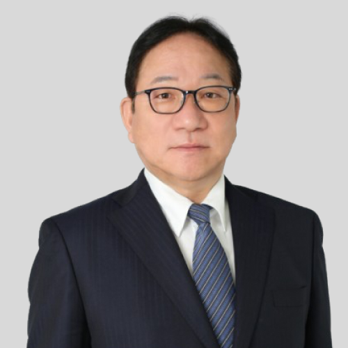
Tadahiro Suhara
TSSC
Education:
・Bachelor, Economics, Doshisha University, Japan, 1983
Experience:
・TSSC, CEO, 2023/5~
・JSR Corporation, Managing Officer, 2019~2023
・Screen Semiconductor Solutions , CEO, 2014~2019
・Dainippon Screen Manufacturing , 1983~2014
Company Profile
TSSC is a consulting company to support Semiconductor and Semiconductor Supply Chain for enabling continuous Semiconductor industry’s growth.

09:00 – 09:20
Opening Speech: Latest Trends in Japan’s Semiconductor Strategy
AI and semiconductors are one of the 17 strategic industries under the growth strategy of the new Takaichi Administration.
Ministry of Economy, Trade and Industry (METI) has been advancing policies based on the Semiconductor and Digital Industry Strategy formulated in 2021 and revised in 2023. In the semiconductor sector, Japan aims to achieve a total domestic semiconductor industry sales of over 15 trillion yen by 2030.
To reach this goal, efforts are underway to secure a robust semiconductor manufacturing base, establish production technologies for next-generation semiconductors including 2nm logic chips, and develop future technologies such as photonics-electronics convergence that have the potential to be game-changers.
This presentation will provide an overview of the latest developments in Japan’s semiconductor strategy, as well as the role of semiconductors in Japan-U.S. relations and strategic investment initiatives.
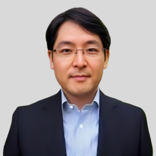
Tomoshige Nambu
Ministry of Economy, Trade and Industry (METI)
Mr. Tomoshige NAMBU has served as the Director for IT Industry Division at the Ministry of Economy, Trade, and Industry (METI) in Japan since July 2025. He leads METI’s AI and semiconductor strategy.
Prior to his current position, he spent 3.5 years in NYC and Washington D.C. from December 2021 to June 2025, serving as Special Advisor for METI at the New York Office of the Japan External Trade Organization (JETRO). He was a senior METI representative in the US, covering trade and economic security policies.
During a more than 20-year career at METI, Mr. Nambu has held responsibilities across a diverse range of public policy areas. He was involved in the formulation of Japan’s economic policy in 2018-2021 as the Director for Macroeconomic Policy at METI. He also assumed the duty of Cabinet Counselor, drafting policy proposals on economic growth strategy under the direction of the Prime Minister’s office.
He was stationed in Washington D.C. as the Trade Attaché at the Embassy of Japan in the U.S. from 2012 to 2015 and worked on several bilateral trade issues such as TPP and energy exports from the U.S.
He joined METI in 2002 after receiving a Bachelor of Law from the University of Tokyo. He also holds an L.L.M from Harvard Law School. He served as the Asia Program Fellow at the Rajawali Foundation Institute for Asia in Harvard Kennedy School in 2009-2010. He currently lives in Tokyo with his wife.
Company Profile
METI has been transforming itself to respond to the needs of the times.
METI has a history of responding to the changing needs of society. Therefore, its history is the history of Japan’s progress.
In 1949, the Ministry of Commerce and Industry was reorganized and the Ministry of International Trade and Industry was established. Its internal subdivisions consisted of eight bureaus: Minister’s Secretariat, Trade Bureau, Trade Promotion Bureau, Enterprise Trade Bureau, Textile Trade Bureau, General Merchandise Trade Bureau, Machinery Trade Bureau, Chemical Trade Bureau, and Iron and Steel Trade Bureau.
In addition, four agencies, the Resources Agency, Small and Medium Enterprise Agency, Industrial Technology Agency, and Patent Office; eight regional trade and industry bureaus; and four regional coal bureaus were established as external subdivisions.

09:20 – 09:40
Keynote
Imaging & sensing technologies to create emotion
Will introduce the latest initiatives of process and device technologies that enhance Sony’s image sensors to create “Emotion.”
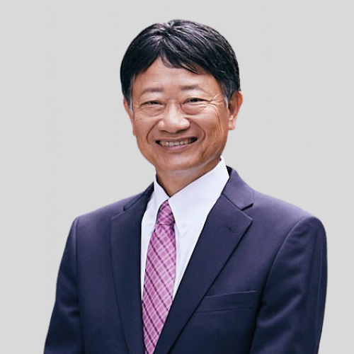
Terushi Shimizu
Sony Semiconductor Solutions Corporation
In April 1980, he joined Sony Corporation (renamed Sony Group Corporation in April 2021), where he served as an engineer in the semiconductor business.
From 1991, he moved to the U.S. to be engaged in planning and control of semiconductor business at Sony Electronics’ Fab.
After returning to Japan, from 1999, he was assigned to Sony Computer Entertainment Inc. as the General Manager of the planning and control department, where he was responsible for the start-up of semiconductors for PlayStation.
In 2016, he was appointed Representative Director and President of Sony Semiconductor Solutions Corporation.
From 2020 to March 31, 2025, he was Representative Director, President and CEO of the company.
From 2021 to March 31, 2025, he was Senior EVP, Officer in charge of Imaging & Sensing Solutions Business, Sony Group Corporation.
He was appointed to Director and Chairman of Sony Semiconductor Solutions Corporation as of April 1, 2025.
Company Profile
Sony Semiconductor Solutions Corporation is a wholly owned subsidiary of Sony Group Corporation and the global leader in image sensors. We strive to provide advanced imaging technologies that bring greater convenience and joy to people’s lives. In addition, we also work to develop and bring to market new kinds of sensing technologies with the aim of offering various solutions that will take the visual and recognition capabilities of both human and machines to greater heights.
09:40 – 10:00
Keynote
The Future of Computing – a future vision of AI for semiconductors
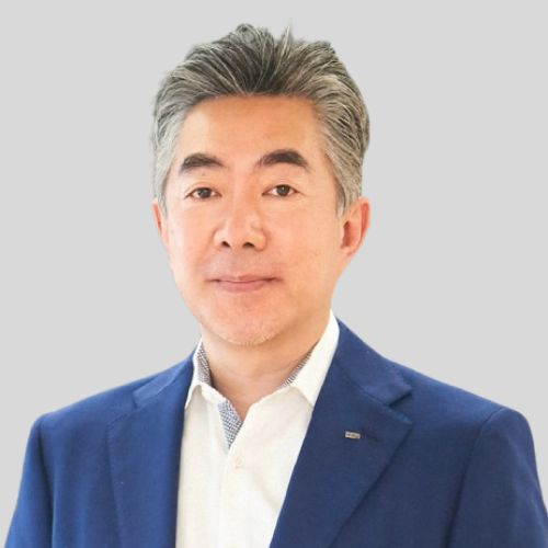
Norishige (Noly) Morimoto
IBM Japan
Norishige Morimoto is Vice President and CTO of IBM Japan, and a Board Member since 2024. He joined IBM in 1987 as a hardware engineer and earned his Master’s in EE&CS from MIT in 1995. He has held global leadership roles including Director of IBM Research-Tokyo, CTO of IBM Asia Pacific, and VP of R&D Japan. He formerly chaired the Information Processing Society of Japan and served on boards of Temple University Japan and SMBC Group. He advises METI’s semiconductor strategy panel and is a member of JAOTEX, promoting innovation and leadership in Japan’s tech ecosystem.
Company Profile
IBM is a leading provider of global hybrid cloud and AI, and consulting expertise. We help clients in more than 175 countries capitalize on insights from their data, streamline business processes, reduce costs and gain the competitive edge in their industries. IBM’s breakthrough innovations in AI, quantum computing, industry-specific cloud solutions and consulting deliver open and flexible options to our clients.
Visit www.ibm.com for more information.
10:05 – 11:05
Networking & Business Meeting 1 + 2
11:10 – 11:30
Keynote
Advancing AI with Energy Efficient Strategies
The ever-growing demand for AI computing power is propelling rapid advancements in packaging technology. AMD is at the forefront of these innovations, leading the way in 2.5D, 3D, and 3.5D packaging technologies. Beyond these advancements, we are pioneering the transformation of packages into complete systems by integrating components such as co-packaged optics. This presentation will delve into the limitations of wafer-scale and explore the emerging trend of panel-scale packages that integrate entire systems. The discussion will emphasize the intersection of architecture, optics, and thermal design, illustrating how these elements converge to meet the increasing demands of high-performance, energy-efficient applications.

Deepak Kulkarni, Ph.D.
AMD
Deepak Kulkarni is a Senior Fellow at Advanced Micro Devices (AMD), where he leads the Instinct and Optics Technology Development team. In this role, he develops heterogeneous architectures for AMD’s AI accelerator products and oversees Photonics technology development.
With twenty years in technology development, Deepak has led the development of several innovative technologies such as panel-level fan-out, Embedded Multi-die Interconnect Bridge (EMIB), Elevated Fan-Out Bridge (EFB), and 3.5D packaging solutions. Recognized with top awards at both AMD and Intel, and a frequent voice on high-level industry panels, Deepak brings both technical depth and strategic vision to advancing heterogeneous integration.
Deepak’s technical interests cover Co-packaged Optics, Panel-level packaging, and design-technology co-optimization. He holds forty patents and has published over twenty papers. He earned his PhD in Mechanical Engineering with a minor in Computational Science from the University of Illinois at Urbana-Champaign.
Company Profile
For 50 years, AMD has driven in high-performance computing, graphics, and visualization technologies – the building blocks for gaming, immersive platforms, and the datacenter. Hundreds of millions of consumers, leading Fortune 500 businesses and cutting-edge scientific research facilities around the world rely on AMD technology daily to improve how they live, work and play. AMD employees around the world are focused on building great products that push the boundaries of what is possible. For more information about how AMD is enabling today and inspiring tomorrow, visit AMD (NASDAQ:AMD) on their website, blog, Facebook and Twitter pages.

11:30 – 11:50
Keynote
Driving the Future of Semiconductor Innovation: AI-Enabled Advanced Nodes and Japan’s Leap Forward
In this keynote, I will explore how AI-driven innovations such as Raads and DMCO are revolutionizing advanced semiconductor nodes and reshaping the future of chip manufacturing. By integrating intelligent design automation and data-centric optimization, these technologies accelerate development cycles and enhance yield. I will also highlight Japan’s strategic leap in semiconductor leadership, including breakthroughs in advanced packaging and ecosystem collaboration. How AI is unlocking new possibilities in scalability, performance, and sustainability—positioning Japan at the forefront of global semiconductor innovation.
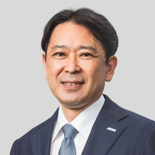
Kazunari Ishimaru, Ph.D.
Rapidus Corporation
Dr. Kazunari Ishimaru, IEEE Fellow, is CTO and Senior Managing Executive Officer at Rapidus Corporation. He began his career at Toshiba in 1988, contributing to SRAM and logic development. As VP of R&D at Toshiba America Electronic Components, he led 32nm–20nm CMOS projects with IBM. Returning to Japan, he oversaw logic manufacturing at Toshiba Oita and emerging memory R&D at Kioxia Yokkaichi, later becoming Director of the Institute of Memory Technology R&D. He joined Rapidus in 2023 and became CTO in 2025, driving Japan’s advanced semiconductor initiatives, including 2nm logic and the RUMS model for integrated manufacturing innovation.
Company Profile
Rapidus will contribute to the fulfillment, prosperity, and well-being of people’s lives through semiconductors. We promote fab management with world-class R&D and manufacturing capabilities, collaborate with universities and research institutions to foster talents vital for semiconductor field, and further innovate toward a truly green society. Based on this corporate philosophy, we will establish new business schemes in cooperation with companies worldwide, develop and provide the world’s best cycle time reduction services, and promote creation of new industries together with our customers.

11:55 – 13:15
LUNCH
13:20 – 13:40
Imec’s nanoelectronics research platform: Collaborative approach for breakthrough innovations
Our life is increasingly guided and supported by semiconductor devices and systems, enabling smart application areas from high-performance computing to health, automotive, industrial automation and robotics. And the massive breakthrough of AI is accelerating this disruptively.
To sustain the momentum, we must rethink upscaling and performance improvements at device, architecture, and system levels. All these roadmaps will face fundamental bottlenecks, with one overarching issue: the energy equation. From grid to chip, the challenges range from delivery, conversion, consumption, and dissipation.
Worldwide approaches in R&D will be required to tackle these challenges and continue the trend toward more efficient systems and growing prosperity. This talk will address a selection of technology solutions that imec is working on to change the needle in the energy equation and will present the collaborative models we propose to realize these innovations.

Lode Lauwers, Ph.D.
imec
Lode Lauwers is Senior Vice President Business Development and Strategy in IMEC, the nanoelectronics R&D Center in Leuven, Belgium. His current focus is to architect new global R&D collaborations and related business models, in line with semiconductor technology initiatives in various continents currently in conception. In that role he also guides imec’s Corporate Business Development strategies in nanoelectronics. Since he joined IMEC in 2005, he had various leading roles in IMEC’s technology business development and partner relation management. He has been driving over 2 decades the build-out, growth and business foundations of imec’s flagship core program with leading IC manufacturers, foundries, equipment and material suppliers and design and system houses. Earlier, he has been general manager of an ASIC design house, part of a US-based ASSP provider for the telecom industry, and scientific advisor for government funding in local and European cooperative networks in micro-electronics and telecommunications. He has a PhD in Electrical Engineering from KU Leuven.
Company Profile
Imec is a world-leading research and innovation hub in advanced semiconductor technologies. Leveraging its state-of-the-art R&D infrastructure and the expertise of over 6,500 employees, imec drives innovation in semiconductor and system scaling, artificial intelligence, silicon photonics, connectivity, and sensing.
Imec’s advanced research powers breakthroughs across a wide range of industries, including computing, health, automotive, energy, infotainment, industry, agrifood, and security. Through IC-Link, imec guides companies through every step of the chip journey – from initial concept to full-scale manufacturing – delivering customized solutions tailored to meet the most advanced design and production needs.
Imec collaborates with global leaders across the semiconductor value chain, as well as with technology companies, start-ups, academia, and research institutions in Flanders and worldwide. Headquartered in Leuven, Belgium, imec has research facilities in Belgium, across Europe and the USA, and representation on three continents. In 2024, imec reported revenues of €1.034 billion.
Further information on imec can be found at www.imec-int.com.

13:40 – 14:00
AI-driven Advanced Packaging – trends, market view and a Japanese perspective

Dimitrios Damianos Ph.D.
Yole Group
Dimitrios Damianos is a Senior Manager for Consulting Services at Yole Group.
With over 10 years of experience in the fields of nanotechnology, semiconductors, market research and strategy consulting, Dimitrios provides strategic insights and tailored solutions/consulting projects to clients across the whole semiconductor value chain and emerging technologies, and is also responsible for commercial & customer relationships.
Dimitrios has successfully managed and authored multiple market reports and client projects, including market analysis, competitive intelligence, marketing/go-to-market studies, technology assessments, strategy, Due Diligence and tech M&A for clients ranging from startups and R&D institutes to Fortune 500 companies and governments.
He holds a BSc in Physics and MSc in Photonics, as well as a PhD in optics & microelectronics.
Company Profile
Yole Group is a leading international market research and strategy consulting firm, delivering in-depth analyses across market trends, technology developments, teardowns, and reverse costing. Leveraging deep semiconductor expertise, its team of analysts also provides custom consulting services, offering strategic, technical, and market insights tailored to address specific business challenges and opportunities.

14:00 – 14:20
New Silicon cycle can be expected
The competition between the US and China is having a major impact on the semiconductor industry. Japan is beginning to have an important position in this industry.
I analyze the impact that investment in advanced packaging technology, which is expected to be the next big technology after chip shrink, and DX, GX, and AI investment lead next silicon cycle .
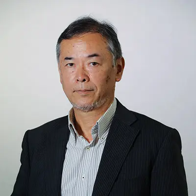
Akira Minamikawa
Informa TechTarget
For 20 years at JEITA, Akira worked as a core analyst for the Global Electronic Devices and Semiconductor Mid- to Long-Term Outlook Committee. Research and consulting in Asia, including regularly giving lectures at semiconductor symposiums hosted in Taiwan. Member of the Japan Patent Office’s technical review committee for automotive patents and semiconductor-related patent review committee.
Member of NEDO’s research evaluation committee for “Development of FeRAM Manufacturing Technology,” a post-5G technology review committee, an outside director at Hakuto, an advisory board member at Mitsubishi Corporation, and an open innovation advisor at the Tokyo Institute of Technology.
Company Profile
Informa TechTarget informs, influences and connects the world’s technology buyers and sellers, helping accelerate growth from R&D to ROI.
With a vast reach of over 220 highly targeted technology-specific websites and over 50 million permissioned first-party audience members, Informa TechTarget has a unique understanding of and insight into the technology market.
Underpinned by those audiences and their data, we offer expert-led, data-driven, and digitally enabled services that have the potential to deliver significant impact and measurable outcomes to our clients:
Informa TechTarget is headquartered in Boston, MA and has offices in 19 global locations.

14:20 – 14:40
The Future of Advanced Package for AI Application
Advances in heterogeneous chip packages are needed to empower today’s device manufacturers to pursue tomorrow’s breakthroughs. Samsung Advanced Package Platform is to be introduced in terms of technology roadmap, challenges and opportunities for emerging high-end computing, memory and mobile applications.

Takashi Kariya, Ph.D.
Samsung
Received PhD in Electronic Engineering from Tohoku university.
1991-2015
Ibiden Corporation
– Management for Package Substrate Development Leaded substrate technology pathfinding with major semiconductor IDM, Fab less, Foundry, OEMs more than 10 years.
2015-2022
TDK Corporation
– Management for Development and business operation of Thin film component and Module. Leaded cutting edge components, MEMS and embedded IC modules.
2022-
Samsung Japan Corporation, Device Solutions R&D Japan
– Head of Advanced Package Lab of Samsung Japan Corporation and also Corporate Vice President of Samsung Electronics Corporation.
– Launch Advanced Package lab in Yokohama and setting up R&D environment at MinatoMirai.
Company Profile
Samsung Electronics Co., Ltd. engages in the manufacturing and selling of electronics and computer peripherals. The company operates through following business divisions: Consumer Electronics, Information Technology & Mobile Communications and Device Solutions. The Consumer Electronics business division provides cable television, monitor, printer, air-conditioners, refrigerators, washing machines and medical devices. The Information Technology & Mobile Communications business division offers handheld products, communication systems, computers and digital cameras. The Device Solutions business division comprises of memory, system large scale integrated circuit and foundry. The company was founded on January 13, 1969 and is headquartered in Suwon, South Korea.

14:40 – 15:00
Memory Bandwidth is All You Need
(Language: Japanese, English interpretation provided)
As generative AI continues to evolve, the importance of inference computing is poised to grow steadily. In this session, the speaker Takahiro Ogura will introduce the 3D-stacked memory structure, a technological breakthrough for AI inference chips, and demonstrate its potential for social transformation through AI agents and edge AI. Ogura will also share his company Preferred Networks’s vision for democratization of AI and creation of new paradigms through their proprietary chip design, ecosystem development and industry collaborations.

Takahiro Ogura
Preferred Networks
Takahiro Ogura is a seasoned leader in high-performance computing with over 20 years of experience. He currently heads the AI Computing Division at Preferred Networks (PFN), overseeing the company’s critical computing infrastructure technologies including the MN-Core™ series of AI semiconductors and in-house supercomputers. Prior to joining PFN, he served as the after-sales service manager for domestic high-performance computing clients at Fujitsu, where he began his career as a systems engineer working on supercomputer systems projects. A notable career highlight was his instrumental role in the design and development of the Fugaku (Post-K) supercomputer at Japan’s national research and development agency RIKEN. Ogura received a Master’s degree from Tsukuba University’s Systems and Engineering program in 2005.
Company Profile
Preferred Networks (PFN) is a leading Japanese AI technology company known for its vertically integrated development of cutting-edge technologies—from custom AI chips, generative AI foundation models to real-world AI solutions and products. PFN plays a key role in advancing Japan’s AI sovereignty and has earned a strong domestic reputation. PFN’s AI solutions span across diverse industries including manufacturing, materials, energy, pharmaceuticals, healthcare, finance, retail, and entertainment. The company is currently developing a novel AI inference chip, leveraging its highly energy-efficient MN-Core™ logic and a new memory technology, with a release targeted for early 2027.
Company Products & Services
Preferred Networks (PFN) develops cutting-edge technologies across the AI value chain from semiconductors, supercomputers, generative AI foundation models to AI solutions and products:
MN-Core™ — a series of highly energy-efficient AI chips, which made a debut topping the Green500 list of the world’s most energy-efficient supercomputers three times in 2020/21. PFN is currently developing a new line of MN-Core chips focused on AI inference, set for release in early 2027.
Preferred Computing Platform™ (PFCP™︎) — a cloud-based service that provides users with access to the computing power of MN-Core 2. PFN has also announced a joint venture with Mitsubishi Corporation and IIJ aiming to launch an MN-Core™-based IaaS commercial service in 2026.
PLaMo™ — a series of Large Language Models developed fully from scratch by PFN, delivering top-tier performance in Japanese-language capabilities. These models power a wide range of AI applications in sectors such as finance, healthcare, and the public sector.
Matlantis™ — a cloud-based, high-speed universal atomistic simulator. Powered by a machine learning interatomic potential (MLIP), Matlantis significantly accelerates the simulation workflow in new materials discovery across industries such as semiconductor, automotive, and energy, by bypassing traditional heavy electronic state calculations.

15:00 – 15:20
Every Watt Matters: How Low-Power Memory is Transforming Data Centers
(Language: Japanese, English interpretation provided)
AI’s explosive growth is driving unprecedented energy demands, making power efficiency the critical challenge for data centers. Tadashi Onodera, Vice President of LPDDR Engineering at Micron, will share how low-power memory technologies—such as LPDDR5X and SOCAMM2—are redefining performance and sustainability. These innovations deliver significant reductions in power consumption while boosting capacity and reliability, enabling scalable AI workloads without overwhelming energy infrastructure. Onodera-san will explore the industry’s energy dilemma, the widening gap between compute and memory bandwidth, and Micron’s commitment to solutions that make every watt count. Attendees will gain insights into how advanced memory architectures can help overcome the power bottleneck, support greener data centers, and unlock the next wave of AI innovation.
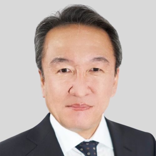
Tadashi Onodera
Micron Technology
Vice President of LPDDR Engineering at Micron, with over 30 years of experience in the DRAM industry. Since joining Elpida in 2003, consistently focused on the design and development of Low Power DRAM (LPDRAM). Currently responsible for the development of all LPDRAM for the Mobile and Client markets at Micron. Previously held various positions with increasing responsibility at Elpida and NEC Corporation.
Company Profile
Micron is a world leader in innovative memory solutions that transform how the world uses information. For over 40 years, our company has been instrumental to the world’s most significant technology advancements, delivering optimal memory and storage systems for a broad range of applications.
15:25 – 16:25
Networking & Business Meeting 3 + 4
16:30 – 16:50
Open Innovation Strategy of Resonac, Co-Creative Chemical Company
The cutting-edge semiconductors necessary for the evolution of AI are supported by advances in equipment and material technology. The emergence of chiplet package structures has led to increased complexity in packaging, making collaboration between materials manufacturers and equipment manufacturers more critical than ever.
Resonac, a co-creative chemical company that provides a variety of semiconductor materials such as CMP slurry, etching gas, materials for HBM, epoxy molding compounds, substrate core materials, and more, is advancing materials technology development through open innovation activities. Resonac has started a Packaging Solution Center to propose one-stop solutions for customers and has established the co-creative packaging evaluation platform “JOINT2” with leading companies to accelerate the development of advanced materials, equipment, and substrates for 2.xD and 3D packages. Furthermore, in 2025, the company launched the open innovation initiative “US-JOINT” in Silicon Valley, USA, and launched a new co-creation platform, “JOINT3,” in Japan to accelerate technology development through co-creation. This presentation will introduce Resonac’s co-creation strategies.

Hidenori Abe
Resonac Corporation
Hidenori Abe is CTO for semiconductor materials and Executive Director of Electronics Business Headquarters at Resonac. He leads R&D and strategy for electronic materials in semiconductors, substrates, and displays. Previously, Mr. Abe served as the head of the Electronics R&D Center and Packaging Solution Center, where he contributed to advanced packaging development through open innovation. Notably, in 2021, he directed the launch of JOINT2, a consortium targeting 2.xD and 3D packaging technologies. He received a master’s degree in chemical engineering from Tokyo Institute of Technology, Japan, and a master’s degree in the Executive MBA program from the University of Oxford, UK.
Company Profile
Resonac defines its purpose as “Change society through the power of chemistry.” Resonac aims to be a world-class functional chemical manufacturer, creating functions necessary for the times, supporting technological innovation, and contributing to the sustainable development of our customers. Resonac is Global Leading semiconductor materials supplier. In order to achieve technological innovation for solving various social issues, it is essential for us to make wide-ranging co-creative efforts with partners, and Resonac is open to collaboration including 1on1 co-development with any partner.
We have opened a Packaging Solution Center and are actively engaged in next-generation semiconductor co-creation activities through JOINT2 with many partner companies. Furthermore, starting this year, we will also seek co-creation opportunities in the United States by launching US-JOINT.

16:50 – 17:00
Interconnects of complex heterogeneous integration structures
Major trend and interconnection technology development direction for complex heterogeneous integration structures

Nelson Fan
ASMPT Semiconductor Solutions
Vice President, Advanced Packaging Product Portfolio Management and Business Development of ASMPT SEMI, is a distinguished leader and innovator with over three decades of impactful contributions to the semiconductor industry. His career is characterized by a unique blend of entrepreneurial vision, deep technical expertise, and a proven track record in senior executive management.
Company Profile
ASMPT Limited, founded in 1975, is headquartered in Singapore and is listed in Hong Kong Stock Exchange since 1989.
ASMPT is the only company in the world that offers high-quality equipment for all major steps in the electronics manufacturing process – from carrier for chip interconnection to chip assembly and packaging to SMT. No other supplier offers a comparable range and depth of process expertise.
Semiconductor Solutions Segment Business of ASMPT offers a diverse product range from bonding to molding and trim & form to the integration of these activities into complete in-line systems for the microelectronics, semiconductor, camera modules, advanced packaging, photonics, and optoelectronics industries.
The group has successfully established itself as the leading player in the back-end assembly and packaging market with its innovative solutions and constant focus on customer value creation.

17:00 – 17:10
TOPPAN’s Challenge in Advanced Semiconductor Packaging
(Language: Japanese, English interpretation provided)
TOPPAN has been active in the FC-BGA business for over 20 years, and particularly in the communication infrastructure sector,such as base stations, where the high-speed transmission characteristics—our core strength—are utilized, and we have accumulated solid experience through continuous use by many customers. Now, driven by the explosive demand of the AI market, semiconductors are strongly required to achieve further enhanced performance and higher integration.With the foresight to recognize this market requirement and change, TOPPAN meets the challenge with our proprietary technology.Specifically, by maximizing the advantages of glass materials and offering next-generation package items based on this as a core technology, we realize solutions that resolve the performance challenges of the rapidly developing AI market.
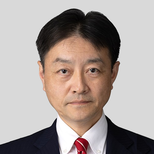
Akihiko Furuya
TOPPAN
(Appointed Dates)
April 1993 Joined Toppan Printing Co.,Ltd., Electronics Division
April 1996 TOPPAN Kumamoto Technical Research Institute.
April 2002 TOPPAN (Corporate) Technical Research Institute
April 2010 General Manager, FC-BGA Engineering Department, Toyama Plant
April 2014 General Manager, FC-BGA Engineering Department, Niigata Plant
April 2018 Head of Technical Development Headquarters Ⅱ, Electronics Division
April 2022 Head of Semiconductor Business, Electronics Division
April 2023 Executive Officer, Head of Semiconductor Business, Electronics Division
October 2023 TOPPAN Inc. Executive Officer, Head of Semiconductor Business, Electronics Division
April 2025 TOPPAN Inc. Executive Officer, Head of Semiconductor Subdivision, Electronics Division
Company Profile
TOPPAN Inc. has grown beyond its traditional printing business and now offers a broad range of products and services with printing technologies at their core in the Information & Communication, Living & Industry, and Electronics segments.
Company Products & Services
Turning printing technologies into leading edge electronics products
Semiconductor-Related(FC-BGA Substrates, Color Filter Arrays, Etched Products, Photomasks/Nanoimprint Molds, LSI Design/LSI Turnkey Service)
Display-Related(Color Filters, TFT LCDs, Surface Treatment Films, Light Control Film)

17:10 – 17:20
Advanced Packaging Solutions with Direct Atomic Layer Processing (DALP®) Technology
Advanced packaging requires new approaches to achieve heterogeneous integration, energy efficiency, and performance scaling beyond conventional methods. ATLANT 3D’s proprietary Direct Atomic Layer Processing (DALP®) technology delivers a breakthrough by enabling localized, maskless material processing with atomic precision. This unique capability provides unmatched flexibility for next-generation packaging architectures, including 2.5D and 3D integration. By combining speed, cost efficiency, and material versatility, DALP® paves the way for transformative advances in semiconductor manufacturing and packaging innovation.

Maksym Plakhotnyuk, Ph.D.
ATLANT 3D
Dr. Maksym Plakhotnyuk, is the CEO and Founder of ATLANT 3D, a pioneering deep-tech company at the forefront of innovation, developing the world’s most advanced atomic-scale manufacturing platform. Maksym is the inventor of the first-ever atomic layer advanced manufacturing technology, enabling atomic-precision development of materials, devices, and microsystems. A scientist with a Ph.D. in Nanotechnology, he has deep expertise in nanotechnologies, renewable and exponential technologies, semiconductor processing, solid-state physics, and material science. A Fulbright scholar, Hello Tomorrow Grand Winner, and proud Ukrainian, Maksym has earned global recognition for his work.
Company Profile
ATLANT 3D has mastered control of matter at the atomic scale, ushering in a new era in manufacturing. For research teams and manufacturers working at the frontiers of technology, we’ve created what was once thought unattainable: a system that builds materials and devices, atom by atom, with unprecedented precision and speed.
While others are constrained by traditional manufacturing limits, our breakthrough technology makes it possible to create the seemingly impossible, from next-generation quantum computers to devices that can operate in the harsh conditions of space. By replacing complex, resource-heavy processes with precise atomic-scale fabrication, we’re transforming technology while making manufacturing sustainable. We’re providing innovative teams the power to build technologies today that will define tomorrow’s world, using fewer resources to achieve greater possibilities.
Based in Copenhagen and London, with operations in the US, ATLANT 3D partners with research institutions and industrial companies to expand the boundaries of technological possibility.
Company Products & Services
ATLANT 3D is redefining microfabrication with its patented Direct Atomic Layer Processing (DALP®) technology. Our NANOFABRICATOR™ platform enables localized atomic layer processing for rapid material discovery, prototyping, and scalable device fabrication—bridging the gap from lab to fab.
Beyond hardware, we offer Pilot Projects and Joint Development Services to validate new materials and device architectures. A-HUB, our Microfabrication-as-a-Service (MaaS) centre, provides R&D teams with atomic-scale precision without the need for costly infrastructure.
From concept to fabrication, ATLANT 3D partners with academia and industry to drive next-generation innovations beyond conventional limits.

17:20 – 17:40
The Digital Sales Room – The Future of Manufacturing Sales
Manufacturers face a rapidly changing sales landscape where digital engagement is no longer optional—it’s essential. This session explores how Product Information Management (PIM), Digital Asset Management (DAM), and Product Experience Management (PXM) transform the way manufacturing companies’ market, sell, and deliver value.
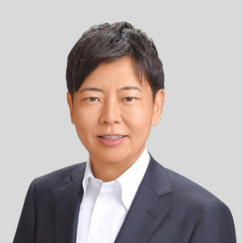
Nobuaki Watanabe
Centric Software
Nobu Watanabe is a seasoned expert in Cloud Computing, API economy, and Product Experience Management (PXM), with over 20 years in the software industry. He co-founded a tech startup in Japan in 2005, led it to IPO, and later established Contentserv Inc. in 2017 as Managing Director. Until March 2025, he spearheaded Contentserv’s growth across APAC, driving digital transformation for manufacturers and retailers with PIM and DAM solutions. Following Centric Software’s acquisition of Contentserv in March 2025, Nobu now leads Centric PXM’s APAC business, continuing to drive innovation, digital strategy, and customer success across the region.
Company Profile
Centric Software® (a subsidiary of Dassault Systemes Group) provides AI-powered platform for consumer goods brands, retailers, and manufacturers of all sizes, covering every process from product ideation to commercialization.
Centric PXM™ (formerly Contentserv) connects product data, digital assets, and content across all channels to accelerate go-to-market execution and deliver consistent, high-quality product experiences worldwide.
Built for industrial-scale efficiency, Centric PXM integrates PIM, DAM, Content Syndication, and Digital Shelf Analytics (DSA) in one unified solution. Manufacturers leverage Centric PXM to streamline product data management, automate content delivery, and gain real-time insights into performance across distributors, e-commerce platforms, and retail partners.
Global leaders in consumer goods and manufacturing achieve measurable results with Centric Software — including up to 400% faster revenue growth, 80% cost reduction in content creation, and an 8.5x increase in product data accuracy.
Part of the comprehensive Centric Software portfolio, Centric PXM complements Centric PLM™, Centric Planning™, and Centric Market Intelligence™, helping manufacturers manage every stage from concept to consumer with full compliance, visibility, and agility.
Empower your teams. Unify your product experience. Transform your growth with Centric PXM.
Learn more about Centric PXM: https://www.centricsoftware.com/centric-pxm/

17:45 – 18:30
Cocktail Reception
18:30 – 18:40
Dinner check-in
18:40 – 21:00
Gala Dinner and Award Ceremony
End of content
End of content