


07:45 – 08:30
Registration

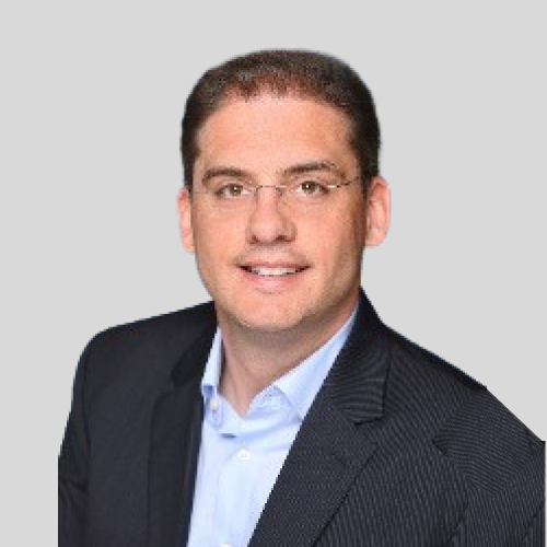
Kamel Ait Mahiout
President
Kamel Ait Mahiout is a seasoned professional with over 30 years of experience in the electronics industry. His expertise spans from RF and Microwave engineering to executive roles in prominent companies such as Unity SC and Amkor Technology, where he significantly contributed to the growth and alignment of the businesses with key industry players.
MEMS Microphone & Speakers
08:45 – 09:05
Keynote
How will Generative AI shape the future of MEMS Microphones?
In the present era, the utilization of AI in diverse applications is steadily increasing, contributing to strength individuals’ efficiency. Tools like ChatGPT play a pivotal role in enhancing people productivity by engaging users through text or voice inputs. Notably, Infineon’s high-performance silicon microphones enable seamless speech interaction with Natural Language Processing assistants. Prior to being processed by Large Language Models, audio data undergoes Speech-to-Text (STT) conversion, a crucial task to ensure accurate input for AI systems. STT operates by breaking down speech into “phonemes” and utilizing spectral comparison to transcribe the audio. Infineon’s initial trials evaluate the significance of high Signal-to-Noise Ratio (SNR) in applications like laptops interpreting the Error Word Rate. Furthermore, in True Wireless Stereo (TWS) and Smart-VR glasses devices, the fusion of AI with Infineon’s Vibration sensor shows the potential to revolutionize current architectures, delivering clear phone calls even any environmental conditions and outperforming current solutions.

Aldo Bruno
Technical Lead MEMS Sensor System Competence Team
Infineon Technologies AG
Aldo Bruno is the Technical Lead MEMS Sensor System Competence Team within the application engineering at Infineon Technologies, specializing in consumer sensors. Before Infineon, he held the role of Digital ASIC Designer at Cirrus Logic UK, where he honed his expertise in DSP, digital filters, audio codec systems, voice activity detection, and speech enhancement algorithms. In 2018, while completing his master’s thesis at Infineon Technologies, he concentrated on the development of ANC systems to explore the potential enhancements Infineon MEMS microphones could bring. Throughout his career and personal pursuits, Aldo’s passion for audio and acoustics has been a driving force since he´s also a musician and music producer.
Company Profile
Here at Infineon, we combine entrepreneurial success with responsible action to make life easier, safer, and greener. Barely visible, semiconductors have become an indispensable part of everyday life. We play a key role in shaping a better future – with microelectronics that link the real and the digital world. Our semiconductors enable efficient energy management, smart mobility, as well as secure, seamless communications in an increasingly connected world. Infineon designs, develops, manufactures and markets a broad range of semiconductors and system solutions. The focus of its activities is on automotive and industrial electronics, communication and information technologies, IoT, sensor technology and security. The product range comprises standard components, software, customer-specific solutions for devices and systems, as well as specific components for digital, analog, and mixed-signal applications.
09:10 – 09:30
MEMS speakers – the ideal earphone tweeters
In this presentation, Jakob will provide an overview of the MEMS loudspeaker industry from USound’s perspective, highlighting interesting trends. A focus will be placed on the potential of MEMS speakers as tweeters in 2-way earphones. Jakob will explain the technical advantages MEMS bring to this specific application and how these advantages benefit the market and ultimately enhance the user experience.

Jakob Spoetl
Head of Acoustics
Usound
Jakob Spötl works as head of acoustics in the R&D department of USound. He is one of the first employees of USound and joined the company in 2015, right after finishing his studies in electrical and audio engineering at the TU Graz in Austria. His main interest was (and still is) the multidisciplinary; combining knowledge from different fields. Therefore, his main expertise lies in understanding and modeling of the interplay between different physical domains (electronics, mechanics, and acoustics). Combining this with real-world applications and the resulting psychoacoustic experience is what he thrives on.
Company Profile
USound GmbH is a fast-growing company that develops advanced audio solutions based on MEMS speaker technology. Headquartered in Austria and with offices in Shenzen, China, USound enables its global customers to bring new revolutionary audio products to the market.
USound is disrupting the audio industry, setting new standards in audio experience. The company achieves this through radical miniaturization, power reduction, and increased production efficiency. USound MEMS speakers are ideal for state-of-the-art TWS earphones, IEMs, audio and AR/VR glasses, OTC hearing aids, and various consumer electronics products. The company’s audio products are safeguarded by over 370 patents.
Leadership:
Ferruccio Bottoni, CEO & Co-Founder
Andrea Rusconi, CTO & Co-Founder
Herbert Gartner, CFO & Chairman
Company Products & Services
USound provides advanced audio solutions based on MEMS technology. USound’s products include MEMS speakers, audio modules, amplifiers, software, evaluation kits and reference designs. USound MEMS speakers, in particular, are distinguished for their small size, lightweight components, and unparalleled audio performance. They are the ideal solution for a wide variety of applications, from TWS earphones and OTC hearing aids to AR/VR glasses and medical devices.

The Role of AI in MEMS and sensors
09:35 – 09:55
It is not only about AI in MEMS and sensors
Sensors have become ubiquitous, blurring the line between being online and offline. AI plays a key role in sensors, enabling real-time context understanding and the ability to make decisions aimed at optimizing and reducing the power consumption of the final device. Sensors are no longer merely for data collection; thanks to AI, they can interact with their environment and significantly contribute to innovation and sustainability.

Tarik Souibes
Product Marketing Director
STMicroelectronics
Tarik Souibes holds a master’s degree in physics and graduated from an engineering school with a specialization in materials dedicated to microelectronics. He joined ST in 1998 as a technical marketing engineer. With more than 26 years of experience at the company, Tarik has held various roles and responsibilities, dealing with a wide range of products including power, analog, and sensors.
Today, Tarik is responsible for product marketing for sensors within the ST MEMS Sub-Group.
Company Profile
At ST, we are more than 50,000 creators and makers of semiconductor technologies mastering the semiconductor supply chain with state-of-the-art manufacturing facilities. An integrated device manufacturer, we work with more than 200,000 customers and thousands of partners to design and build products, solutions, and ecosystems that address their challenges and opportunities, and the need to support a more sustainable world. Our technologies enable smarter mobility, more efficient power and energy management, and the wide-scale deployment of cloud-connected autonomous things. We are committed to achieving our goal to become carbon neutral on scope 1 and 2 and partially scope 3 by 2027. Further information can be found at www.st.com.

10:00 – 10:20
MEMS Breaks Through the AI Bottleneck
AI serves as the computational brain for advanced electronic applications, requiring high-quality sensory data to interact effectively with the environment. Emulating sophisticated sensory systems at a micromachined scale, MEMS technologies bridge this gap to enhance AI’s potential. Current advancements in MEMS — particularly in areas such as 3D LiDAR sensors, tactile sensors for robotics, and high dynamic range microphones —are pivotal in overcoming common AI bottlenecks. Additionally, MEMS integration can streamline neural networks, facilitating more efficient AI workflows. This talk will explore how MEMS technologies address crucial performance, reliability, stability and cost issues, thereby opening new market opportunities and significantly impacting future industry trajectories. We will also discuss how MEMS mitigates the power and thermal challenges posed by increasingly powerful and energy-intensive GPUs.

Eric Aguilar
Chief Executive Officer
Omnitron Sensors
An award-winning entrepreneur, Eric Aguilar is a visionary leader in the field of advanced sensor systems for complex systems, such as robotics and autonomous platforms.
Throughout his distinguished two-decade career, Eric’s passion for sensor design and innovation has made him a key player in the industry. His expertise includes leading teams at renowned companies such as Tesla, where he managed a crew of 300 engineers on the firmware for Model 3, and at X, where he spearheaded the development of Google Project Wing, an autonomous drone delivery service.
Eric’s expertise in sensor integration includes leadership positions at autonomous vehicle and robotics companies. His role in steering product development for a sensor company later acquired by Google — as well as for his pioneering work building sensors for drones at US Navy Research Labs — further showcases his depth of experience.
Eric earned a BS in Electrical Engineering from California State Polytechnic University and has pursued advanced studies in Electrical and Electronics Engineering at the University of Southern California. His work continues to shape the future of MEMS and sensor technology, making him a sought-after thought leader and speaker in the field.
Company Profile
Omnitron Sensors is rewriting the script on building high-performance low-cost sensors for the world of tomorrow. Leveraging its executive team’s extensive experience designing, fabricating, and using MEMS sensors, Omnitron has developed a “new topology for MEMS” that addresses some of the most pressing pain points in MEMS manufacturing.
Featuring the clever arrangement of silicon process steps and a new packaging method, Omnitron’s topology significantly improves performance to produce robust, rugged, reliable, repeatable, and low-cost MEMS sensors in high volumes by leveraging commercial MEMS foundries.
The company’s first proof point of its new topology for MEMS is a large, robust, low-cost, MEMS scanning mirror for long-range LiDAR.
10:25 – 11:25
Networking Break, Coffee and Business Meetings
AR/VR
11:30 – 11:50
Keynote
MEMS in AR/VR
As Augmented Reality (AR) and Virtual Reality (VR) devices continue to mature, the need for lower size, weight, and power (SWaP) components will only increase. One solution to this demand is with Micro-Electromechanical Systems (MEMS). MEMS devices have become ubiquitous within the consumer electronics industry, and their unique balance of SWaP and performance present a unique opportunity to address the challenges associated with AR/VR development.
In this talk, I will introduce the AR/VR technology space and discuss multiple ways in which the sensing and compute demands push beyond previous methods of interacting with digital content. Current MEMS integration within these devices will be highlighted along with the constraints and opportunities for future MEMS integration.

Ken Diest
Research Manager and Tech Lead
Meta
Ken Diest is a Research Manager and Tech Lead at Meta’s Reality Labs, where he leads programs focused on MEMS and micro-actuator technologies. His focus is on developing these technologies from early stage through production to address critical opto-mechanical and display challenges in AR/MR.
A Materials Scientist by training, Ken’s prior work focused on tunable devices and materials with an emphasis on optical systems. He was the editor and co-author of the book Numerical Methods for Metamaterial Design, and has previously held technology development roles at Apple, MIT Lincoln Laboratories, and Northrop Grumman that focused on new displays and nano-photonics.
Company Profile
Meta builds technologies that help people connect, find communities, and grow businesses. When Facebook launched in 2004, it changed the way people connect. Apps like Messenger, Instagram and WhatsApp further empowered billions around the world. Now, Meta is moving beyond 2D screens toward immersive experiences like augmented and virtual reality to help build the next evolution in social technology.
Automotive
11:55 – 12:15
Advance Packaging for Automotive MEMS and Sensors
Automotive MEMS based Actuator / Sensor and Optical Sensor devices continue to enable new exciting functionalities and applications in the automotive market — in Safety, Entertainment, Passenger Convenience and Advance Driver Assistance Systems (ADAS).
Increasing autonomous levels in the Automotive market requires higher performance for positioning and localization, inertial navigation and object detection / recognition while meeting government recommended or mandated implementation dates. These new functions and applications require more Advance Packaging Technologies, Heterogenous integration and Standard platforms.
The MEMS and Sensor Industry is evolving from a discrete single MEMS/sensor (leadframe + wirebond based packages) towards new packaging and interconnection technologies – such as a new standard Optical Packaging Platform or the use of Cu Pillars to interconnect devices. And increasing complexities require closer collaboration between the different stakeholders in the MEMS Actuator / Sensor and Optical Sensor Ecosystem.
Stefan Martens
Sr Director, MEMS and Sensor BU
Amkor Technology, Inc.
Stefan joined Amkor Technology in 2019 and currently serves as a Senior Director for MEMS and Sensor Products. He manages assembly and test services for large volume automotive and consumer MEMS sensors for European customers. Stefan has 18 years of experience in the semiconductor industry and held positions at Infineon and Huawei in Germany, primarily in the field of RF devices and modules prior to joining Amkor. He has been issued 15 patents and holds a MSc in Applied Physics as well as a PhD in Microsystem Engineering from the University of Freiburg, Germany.
Company Profile
Amkor Technology, Inc. is the world’s largest US headquartered OSAT (outsourced semiconductor assembly and test). Since its founding in 1968, Amkor has pioneered the outsourcing of IC packaging and test services and is a strategic manufacturing partner for the world’s leading semiconductor companies, foundries, and electronics OEMs. Amkor provides turnkey services for the communication, automotive and industrial, computing, and consumer industries, including but not limited to smartphones, electric vehicles, data centers, artificial intelligence and wearables. Amkor’s operational base includes production facilities, product development centers and sales and support offices located in key electronics manufacturing regions in Asia, Europe and the United States. Learn more at https://amkor.com
12:20 – 12:40
Advances in MEMS Sensors & Technologies
• MEMS based sensors are a key-enabler in a wide range of applications: from automotive, over consumer to the life science domain. MEMS is expected to even further proliferate in everyday life, due to their continued miniaturization, steady increase in performance and the accessibility of new sensing functionalities.
• This is possible due to a constant high level of innovation in e.g., processing and packaging technologies, as well as due to novel system-level concepts. This shows the need for an overarching approach, integrating all development domains.
• In his presentation, Dr. Ando Feyh (MEMS Strategy Management, New Business and M&A), will cover a brief review and compare this to the progress achieved by recent advancements in the field of MEMS based sensors. Several examples from above outlined domains will be discussed for illustration.
Dr. Ando Feyh
MEMS Strategy Management, New Business and M&A
Bosch
Ando Feyh received his PhD degree in Electrical Engineering at RWTH Aachen University after a Physics Diploma degree at Stuttgart University.
He started his career at Bosch in 2002 within Corporate Research and Advance Engineering. Concentrating in the field of microsystems, he worked on integration and miniaturization of MEMS sensors, in development and in project management positions.
Between 2010 and 2014 he was an expat in the Silicon Valley in Palo Alto, leading different MEMS projects and an engineering group for MEMS pre-development.
2014 he joined the Bosch internal IoT startup “Bosch Connected Devices and Solutions”, first responsible for Advance Engineering and System Architecture, later as Head of Engineering. Mid 2018 he was nominated Head of Technical Responsibility / CTO, responsible for engineering, project management and product management of IoT devices.
Since mid 2021 he is focusing on MEMS Strategy Management, New Business and M&A projects within the Mobility Electronics Sensors Business unit.
Company Profile
The Bosch Group is a leading global supplier of technology and services. It employs roughly 428,000 associates worldwide (as of December 31, 2023). According to preliminary figures, the company generated sales of 91.6 billion euros in 2023. Its operations are divided into four business sectors: Mobility, Industrial Technology, Consumer Goods, and Energy and Building Technology. As a leading IoT provider, Bosch offers innovative solutions for smart homes, Industry 4.0, and connected mobility. Bosch is pursuing a vision of mobility that is sustainable, safe, and exciting. It uses its expertise in sensor technology, software, and services, as well as its own IoT cloud, to offer its customers connected, cross-domain solutions from a single source. The Bosch Group’s strategic objective is to facilitate connected living with products and solutions that either contain artificial intelligence (AI) or have been developed or manufactured with its help. Bosch improves quality of life worldwide with products and services that are innovative and spark enthusiasm. In short, Bosch creates technology that is “Invented for life.” The Bosch Group comprises Robert Bosch GmbH and its roughly 470 subsidiary and regional companies in over 60 countries. Including sales and service partners, Bosch’s global manufacturing, engineering, and sales network covers nearly every country in the world. The basis for the company’s future growth is its innovative strength. At 136 locations across the globe, Bosch employs some 90,000 associates in research and development, of which roughly 48,000 are software engineers.
12:45 – 13:45
Lunch
13:50 – 14:10
Keynote
Transforming Automotive Interfaces with UltraSense Systems’ Cutting-Edge Monolithic Silicon/PMUT Technology
At UltraSense Systems, we’re at the forefront of revolutionizing automotive touch interfaces with our state-of-the-art HMI Controller solutions and innovative In-Plane Sensing approach. Our advanced monolithic silicon/PMUT technology turns ordinary surfaces into highly responsive, solid surface touch interfaces, delivering an unparalleled driving experience. In today’s automotive industry, touch user interfaces are crucial for modernization and product differentiation.
Our groundbreaking multi-mode touch and force fusion sensing capabilities, enhanced by AI and Machine Learning algorithms, enable virtually any surface of any material (metal, glass, fabric,..) within a vehicle to function as an intuitive touch interface. At the core of our offerings is the smart-solid-surface Human Machine Interface (HMI) controller, which provides customizable features such as audio, illumination, haptics, and user feedback, all designed to elevate the driving experience. By replacing mechanical interfaces with intuitive Smart-Solid Surfaces using our PMUT technology platform, UltraSense enhances both automotive interior and exterior modernization, providing a cost-effective advanced tactile sensing/HMI solution for automotive OEMs.
Mo Maghsoudnia
Founder & CEO
UltraSense Systems
Mo Maghsoudnia is the visionary Founder and dedicated CEO at the helm of UltraSense Systems, a pioneering company in the technology and manufacturing sector. With a track record of transformative leadership and innovation, Mo has been instrumental in shaping the industry landscape.
Before founding UltraSense, Mo Maghsoudnia made significant contributions as the Vice President of Technology & Manufacturing at InvenSense. In this influential role, he oversaw global operations and spearheaded the development of cutting-edge Process Technology. Under his guidance, InvenSense achieved remarkable success, culminating in its acquisition by TDK for a staggering $1.4 billion in 2017.
Prior to his tenure at InvenSense, Mo Maghsoudnia served as the Vice President of Manufacturing at NetLogic MicroSystems. Here, he demonstrated his exceptional ability to steer manufacturing operations, elevating the company from a single product line to a diversified product portfolio powerhouse. His adept leadership, combined with a diverse product range, paved the way for Broadcom’s acquisition of NetLogic MicroSystems for a
remarkable $4 billion in 2012.
Mo’s expertise is firmly rooted in his academic pursuits, holding a Master of Science in Electrical Engineering from Santa Clara University. His passion for innovation is further underscored by his impressive intellectual property portfolio, boasting 12 patents, and an extensive list of research papers that he has authored.
Mo Maghsoudnia’s unwavering commitment to technological advancement and his exceptional leadership have left an indelible mark on the tech and manufacturing sectors, solidifying his status as a true industry luminary.
Company Profile
UltraSense Systems is pioneering the next generation of human–machine interface intelligence, built on its proprietary ultrasound and piezoelectric platform that fuses sensing, haptics, and edge processing into compact, solid-state systems. Its multimodal sensor-fusion architecture—integrating touch, force, ultrasound, lighting, and haptic feedback—creates a unified tactile interface layer that transforms how users interact with devices and environments. The company’s silicon and systems portfolio enables software-defined smart surfaces that operate across diverse materials and form factors, delivering the responsiveness, precision, and design freedom demanded by advanced mobility and next-generation consumer electronics. In automotive, UltraSense Systems powers intelligent cabin interfaces that integrate sensing, actuation, and illumination into seamless surfaces for a futuristic in-cabin experience. In high-end consumer devices, including smartphones and AR glasses, its solutions enable thinner, more immersive, and spatially aware user experiences. Built on deep expertise in ultrasound physics, MEMS, and mixed-signal ASIC design, UltraSense Systems is extending its technology platform into new domains where tactile perception and spatial awareness will define the next era of user experience—combining precision sensing, embedded intelligence, and solid-state reliability to bridge the physical and digital worlds. For more information, visit www.UltraSenseSystems.com.
Company Products & Services
UltraSense Systems delivers the most advanced solid-state HMI technology for the next generation of user interfaces. Our TouchPoint™ family of silicon controllers integrates multi-modal sensing — ultrasound, capacitive, and piezoelectric — with lighting, haptic feedback, and on-chip intelligence.
From TouchPoint C (CapForce™) to Z (UltraForce™), Q (TapForce™), and Edge, each device fuses sensing, control, and communication into a single SoC — enabling touch and force interaction through metal, glass, fabric, and composite surfaces.
Complemented by our UltraSwitch™, UltraSlide™, and UltraTouch™ system modules, UltraSense provides a full-stack platform that transforms static surfaces into intelligent, software-defined interfaces — powering the future of automotive, AR glasses, and high-end consumer devices.
UltraSense Systems — The Future of Solid-State HMI
| Layer | Offering | Description |
| Silicon Platform | TouchPoint™ HMI Controllers | Multi-mode SoCs integrating touch + force sensing, lighting, haptics, and AI-based algorithms |
| C – CapForce™ | Capacitive + Force sensing controller | |
| Z – UltraForce™ | Ultrasound + Force sensing controller | |
| Q – TapForce™ | Piezoelectric Force sensing controller | |
| Edge – Cluster/Slider | Multi-channel HMI SoC with Neural Touch Engine™ + LIN | |
| System Modules | UltraSwitch™ / UltraSlide™ / UltraTouch™ | Complete smart-surface solutions integrating sensing, feedback, and lighting |
| Applications | Automotive • AR Glasses • Consumer Devices | Solid-state, software-defined interfaces that modernize the user experience |
14:15 – 14:35
Industrialization challenges for advanced packaging in foundry environment
(Virtual Presentation)
MEMS process sequences and capabilities are frequently reused for advanced packaging and 3D integration applications. Bringing these to market presents multiple technology and business model challenges. This presentation will discuss progress and future trends.

Volker Herbig
VP BU Microsystems
X-FAB
Volker Herbig, VP BU Microsystems at X-FAB, oversees all MEMS activities within the X-FAB Group. Before assuming his current role, Volker worked as Director Product Marketing at X-FAB. Previously he held also engineering, marketing and management positions at Siemens, Inkjet Technologies and Carl Zeiss where, among other activities, he developed MEMS inkjet print heads and was responsible for setting up a manufacturing facility for those. Volker Herbig holds a master’s degree in physics from Humboldt University, Berlin, Germany.
Company Profile
X-FAB is one of the world’s leading specialty foundry groups for analog/mixed-signal semiconductor technologies with a clear focus on automotive, industrial, and medical applications. As a pure-play foundry, X-FAB provides manufacturing and design support services to customers that design analog/mixed-signal integrated circuits (ICs) and other semiconductor devices for use in their own products or the products of their customers. Its customers worldwide benefit from the highest quality standards, manufacturing excellence and innovative solutions by using X-FAB’s modular CMOS and SOI processes in geometries ranging from 1.0 µm to 110 nm, and its special micro-electro-mechanical systems (MEMS) processes. X-FAB is also the first pure-play foundry to provide comprehensive processing technologies for the wide-bandgap materials silicon carbide (SiC) and gallium nitride (GaN). The GaN-on-Si wafers are manufactured in its modern 8” fab in Dresden, Germany, and SiC wafers in the 6” fab in Lubbock, Texas, USA. X-FAB runs six production facilities in Germany, France, Malaysia and the U.S. The company employs about 4,200 people worldwide.
14:40 – 15:00
The Sensorization of the Modern Vehicle
Vehicles have undergone remarkable changes over the last decades, with semiconductor sensor content increasing dramatically in recent years as more safety and comfort applications are implemented in today’s cars. These sensors need to fulfil their performance requirements whilst concurrently being able to meet stringent automotive reliability criteria – and achieve this in small form factors, adequate cost levels, and with fast time to market. This poses significant challenges to sensor packaging and testing facilities, especially when considering that sensor packages can differ significantly and the package itself is a major contributor to the sensor performance. In this presentation, we will look at how vehicles have evolved to become the collection of sensors they are today, discuss some of the key sensor applications and package structures used for said applications, and give some perspective of packaging trends observed for the next generation of automotive sensors.

Alastair Attard
Director of Business Development
UTAC Group
Alastair Attard is Director of Business Development at UTAC Group. He has a Bachelor’s degree in Mechanical Engineering and an Executive MBA, and brings over 19 years of experience in the semiconductor assembly & test.
Alastair has previously held positions at STMicroelectronics in MEMS and SiP process engineering and package development, and at Besi where he managed the process development group for advanced die attach technologies.
Alastair joined UTAC in 2018 and today is responsible for business development of semiconductor assembly and test solutions with particular focus on MEMS, Sensing, and Advanced Packaging.
Company Profile
UTAC Group is a leading outsourced semiconductor assembly and test (OSAT) provider, founded in 1997 and headquartered in Singapore. The company specializes in advanced assembly and test services for logic, memory, analog/mixed-signal, image sensors, MEMS, and power devices. UTAC supports a global customer base that includes fabless companies, integrated device manufacturers (IDMs), and wafer foundries.
With ten manufacturing facilities across Singapore, Thailand, China, and Indonesia, and a robust global sales network spanning North America, Europe, Greater China, Japan, and Southeast Asia, UTAC delivers comprehensive turnkey solutions—from wafer probing to final testing.
UTAC serves diverse market segments including automotive, computing, communications, consumer electronics, and industrial applications. Renowned for its reliability, technological expertise, and customer-centric approach, UTAC continues to play a vital role in enabling next-generation semiconductor innovation.
Company Products & Services
UTAC Group provides a comprehensive range of semiconductor assembly and test services, delivering turnkey solutions from wafer probe to final test across key end markets.
Its packaging portfolio includes leadframe-based packages such as QFN, DFN, QFP, TLA, and Cu-clip variants, as well as laminate-based BGA/iBGA packages for mobile, computing, and automotive applications. UTAC also offers System-in-Package (SiP) modules that integrate multiple components into compact, high-density solutions for IoT, wearables, and automotive electronics.
Advanced wafer-level offerings include bumping services and Wafer-Level Chip Scale Packaging (WLCSP) for customers requiring miniaturization, high electrical performance, and low-profile form factors.
UTAC also supports image sensor packaging, including automotive-grade iBGA with cleanroom assembly to meet stringent reliability and contamination standards.
To complement mass production, UTAC provides value-added services such as package design support, reliability qualification, and failure analysis—helping customers accelerate time to market with confidence.
15:05 – 15:50
Networking Break, Coffee and Business Meetings
IoT Industries
15:55 – 16:15
Advance CMOS technology to unleash the full power of MEMS sensor
This talk focuses on the cutting-edge developments in CMOS technology that are revolutionizing the capabilities of MEMS sensors. By exploring the synergies between CMOS technology and MEMS sensors, this talk sheds light on the transformative potential of neuromorphic and sensor fusion in pushing the boundaries of sensor technology. Through the implementation of edge AI methodologies, we will also show you the improvement in the following aspects:
- AI in sensor: neuromorphic and sensor fusion have been proven as an effective approach to improve the sensor performance while achieving the low power consumption requirement for wearable products. We will showcase our latest result with AI integrated sensors.
- Privacy for always-on sensor: with the increasing need of 24/7 health monitoring, RF radar has been proposed by industry partners to replace optical and acoustic sensors. During this talk, we will give a performance and cost comparation from the foundry’s point of view.
- Challenge in biosensor: with the increasing computing functions integrated into biosensor, many devices are moving from legacy node to advanced CMOS technology. Major challenges to combine advanced CMOS with microfluidics emerged. In this talk, we will proposal a call for action to resolve this issue.
- Internet of Medical Things: with the rise in digital therapeutics and at-home diagnostics, we see the need to improve foundry quality control to address such mid-risk medical devices with function safety and root-of-trust approach.
Ruby Yan, Ph.D.
Business Unit Director – Display, Sensor, Security
GlobalFoundries
Ruby Yan is a seasoned Business Line Director at GlobalFoundries, where she oversees the Sensing & Display, ID & Security business lines. With over a decade of experience in the company, she has held various roles and responsibilities including technology development and product management. Ruby is not only a Master Inventor with more than 20 patents and over 70 peer-reviewed publications to her name but also a fervent advocate for diversity and inclusion in the tech world. She earned her Ph.D. in Microelectronic Engineering from the National University of Ireland, Cork, and an EMBA from ESCP Business School.
Company Profile
GF is one of the world’s leading semiconductor manufacturers and the only one with a truly global footprint. We are redefining innovation and semiconductor manufacturing by developing feature-rich process technology solutions that provide leadership performance in pervasive high growth markets. As a steadfast partner, with a unique mix of design, development and fabrication services, GF works collaboratively alongside our customers to bring a broad range of innovative products to market. With a global customer base, a talented and diverse workforce and an at-scale manufacturing footprint spanning three continents, GF is delivering a new era of more.

MEMS Testing
16:20 – 16:40
Ensuring Performance and Accuracy: Production Testing Strategies for Next-Generation Environmental Sensors
This presentation delves into the critical world of production testing for MEMS environmental sensors. As these devices play a pivotal role in the environmental monitoring in many situations (from industry, to homes, to hospitals), ensuring their correct performance is of vital importance. Manufacturers face several challenges in guaranteeing the accuracy and reliability of their sensors, whose production testing can be a complex and time-consuming process. As these devices are sensitive to multiple environmental factors and respond to various stimuli (pressure, temperature, humidity, gas, …), the key thing about their testing resides in the need to develop testing setups able to capture all the electrical and mechanical aspects of the sensor, simulating and controlling a multiplicity of environmental factors. The sensor-type specificities represent a second challenge: each sensor type might require unique testing procedures and hardware setup, and this customization can be time-consuming and costly. Finally, while many applications are requiring more accurate and sensitive devices (that means, very accurate test equipment too), achieving high-volume production requires test cost efficiency. We will showcase how the latest advancements in test equipment are revolutionizing the approach for MEMS environmental sensors, solving all these challenges.
Marco Pratillo
Sales Manager Semi & MEMS Test Equipment BU
SPEA S.p.A.
Marco Pratillo received his M.S. degree in Electrical Engineering from the Polytechnic of Turin (Italy) in 2012. He promptly joins SPEA as part of the Product and Test Engineering Group in Electronic Industries and Custom Semiconductor Test Equipment. Starting from 2017, he relocated to Suzhou (China) as Test Engineering Manager Mems and Power Semiconductor, where he contributed to the exponential growth of the Semiconductor Division, Power and MEMs. He spent five years working closely with the Sales team aiming to affirm and expand the presence of SPEA’s products. In 2022, Marco returned to Italy in the role of Technical Sales Manager, specifically dedicated to the biggest Semiconductor manufacturing leaders in Asia.
Company Profile
Established in 1976, SPEA is a world leading company in the field of automatic test equipment for ICs, MEMS, sensors, electronic boards. SPEA serves the big semiconductor IDMs and OSATs with the most cost-effective and high-performance equipment to test automotive, SoCs, analog mixed-signal devices, MEMS sensors and actuators, power and discretes, identification devices, delivering highest measurement capabilities, lowest cost of test and fastest time-to-market. SPEA systems are designed to detect any possible defect in electronic products, so that they won’t fail on the field. High throughput, best detection capability, test techniques designed on the latest technologies requirements, complete configurability. For SPEA customers, testing is not an additional cost, but a tangible competitive advantage.
Company Products & Services
- SPEA product portfolio includes test equipment for:
- Automotive, linear, analog mixed signal & SoC devices requiring the most advanced and powerful instrumentation. SPEA’s DOT platform addresses today’s and future roadmap needs.
- MEMS & Sensors. SPEA has been chosen by the biggest players in this market to develop the best solutions for inertial, high-g, proximity, time-of-flight, light, pressure, environmental, magnetic, acoustic sensors. SPEA equipment combines physical stimulus with a complete electrical test, fast pick&place handling, reliable contacting, tri-temp.
- Power & Discretes. DOT800 T perforfms static and dynamic measurements with extended current/voltage ranges, on the whole range of power applications: wafers, discretes (Si, SiC, GaN based), IPMs, KGDs, DBCs, IGBT modules.
- Identification. CT1000 and CT3000 are low-cost test systems dedicated to micro-controllers, RFID, UHF, combi devices. They perform complete, highly accurate measurements, offering high throughput, with high multi-site test capability at wafer test, and a fast data transfer for memory test.

Transforming Manufacturing
16:45 – 17:05
New Foundry MEMS Ecosystem Accelerator
InchFab offers a new approach to MEMS foundries. It gives the MEMS industry a low cost and fast cycle time microfab service solution designed for today’s microfabricated technologies, addressing the needs of the bio, medical, IoT, aerospace and industrial sensing markets. At InchFab, we enable rapid, cost- efficient development and rapid, low risk scaling to production for today’s emerging technologies. InchFab’s low capex approach to foundry expansion will be discussed as will the ability of InchFab to assist regions wanting to quickly develop their semiconductor infrastructure.
Doug Sparks
Vice President Business Development
InchFab
Doug Sparks is the InchFab VP of business development. He is also the president of M2N Technology, the former CTO of Hanking Electronics and founder and president of NanoGetters. Doug has been in the MEMS indistry for over 3 decades in a variety of roles from startups to management, process, design and packaging.,
Company Profile
InchFab pioneered Application Specific Fabs for the new era of chips, delivering the world’s only drop-in, ready-to-use modular fabrication lines with as short as 6-month delivery lead times. These $1-10M agile fabs enable state-of-the-art wafer processing at a fraction of traditional $1B+ costs. The company provides complete solutions including turnkey process flows, comprehensive education courses, and foundry services. By combining low CapEx, scalable throughput, and a proprietary process library, InchFab democratizes semiconductor manufacturing for workforce development, rapid prototyping, and production across specialized chips, non-IC devices, and localized supply chains.RetryM
Company Products & Services
Application Specific Fabs
17:10 – 17:25
Transforming Industrial Manufacturing: Harnessing the Potential of Ultra High Viscosity Jetting for Functional Printing
The potential to transform industrial manufacturing lies in jetting ultra high viscosity fluids, merging the scalability, flexibility, and digital printing capabilities of NovoJet inkjet technology with the superior properties of functional materials. The ability to jet ultra high viscosity fluids via drop-on-demand inkjet, surpassing previous standards, was first announced by Borrell et al. in 2021. Initially, only small printheads with limited commercial capabilities had been developed and tested, with a tentative specification for a commercial printhead anticipated. Over the past three years, substantial progress has been made in optimizing the underlying actuator technology, enabling jetting of fluids with viscosities up to 250 mPa·s for Newtonian fluids. NovoJet technology is poised to revolutionize applications in fuel cells, printed electronics, MEMS, semiconductors, and more.

Ramon Borrell
CTO
Quantica
Ramon Borrell is a highly experienced professional in the field of Inkjet and industrial printing systems, with 30 years of experience in the industry. He has held technical leadership and executive positions for 20 years, including 14 years at HP where he led the development of large format printers and 14 years as CTO and R&D Director at Xaar, a leading company in inkjet printheads. In 2021, Ramon joined Quantica as CTO, bringing his extensive technical expertise and leadership experience to the company.
Company Profile
Quantica is an advanced additive manufacturing company headquartered in Berlin and Barcelona. Their groundbreaking inkjet-based technology, NovoJet™, transforms production by enabling the digital deposition of high-viscosity and high particle-loaded materials. With their advanced systems, users can print and combine new materials seamlessly in a single process for 2D and 3D application development. From car coatings to printed electronics to hearing aids, Quantica’s technology offers a solution.
Company Products & Services
NovoJet™ JetPack: Empowers researchers and material developers to optimize and validate new materials for NovoJet™ printheads. Future pattern printing and production integration offerings.
NovoJet™ OPEN: An inkjet-based benchtop printer with the unique capability to combine high viscosity materials.
Material validation and optimization training and service offerings available.
Optical Sensing
17:30 – 17:50
Illuminating and complementing: Light-Based Sensing
Light-based sensing technologies have enabled and improved wide range of use cases. This presentation explores the foundational technologies, working principles and building blocks of light-based sensing and actuating. The focus is on specific use case values coming from consumer applications. Key technologies include specialization for light sensing of semiconductor, package, and system architecture including software. Complementing and competing technologies, such as radar and ultrasonic are also discussed. The presentation concludes with a call for industry collaboration to unleash the value of light- sensing in attractive verticals.

Dr. Roland Helm
Senior Vice President, Head of Integrated Optical Sensing
ams OSRAM
Roland joined ams Osram in January 2024, as Senior VP, Heading the Business Line Integrated Optical Sensors. He has a track record in the semiconductor and sensors industry spanning 20 years where he held various leadership positions. In his previous role, he has grown a MEMS business from technical feasibility to technology and market leadership. Before he was working in a technology start-up and in a business consultancy. He is passionate to capture the value of new technology matching the needs of modern society. Roland lives with his family with three kids in Munich. He enjoys time with his family, endurance sports, skiing and sailing.
Company Profile
At ams OSRAM, we pioneer differentiating light and sensor solutions. Looking back on more than 110 years of industry experience, we combine engineering excellence and global manufacturing capabilities with passion for cutting-edge innovation. Our commitment to pushing the boundaries of illumination, visualization, and sensing has earned us the trust of customers worldwide. Together, we create break-through applications that make our world safer, smarter, and more sustainable.
“Sense the power of light” – our success is based on our deep understanding of the potential of light. We harness its full spectrum – visible and invisible – to illuminate our surroundings as well as gather information from them. By adding intelligence to light, we enable our customers to drive transformative applications.
Our around 19,700 employees worldwide focus on innovation alongside the societal megatrends of digitalization, smart living, energy efficiency, and sustainability. Our light and sensor technologies are setting industry standards in the automotive, industrial, medical and consumer electronics markets. This is reflected in our global portfolio of some 13,000 patents and patent applications. Headquartered in Premstaetten/Graz (Austria) with co-headquarters in Munich (Germany), the group achieved EUR 3.4 billion revenues in 2024.
Company Products & Services
Our distinct portfolio of advanced light and sensor technologies sets us apart in our industry. It includes high-quality semiconductor-based light emitters, sensors, CMOS ICs and software as well as a range of traditional lighting technologies for automotive and special applications.
18:00 – 19:45
Cocktail Reception
19:45 – 21:45
Gala Dinner
Advisory Board Recognition
Industry Awards
Entertainment
End of content
End of content