9-11 December 2025
Muscat, Oman
No posts
07:50 – 08:30
Registration

Kamel Ait Mahiout
Kamel Ait Mahiout is a seasoned professional with over 30 years of experience in the electronics industry. His expertise spans from RF and Microwave engineering to executive roles in prominent companies such as Unity SC and Amkor Technology, where he significantly contributed to the growth and alignment of the businesses with key industry players.
09:00 – 09:30
Keynote
Chiplet Ecosystem Acceleration
The speaker will share the work of TSMC in Chiplet Ecosystem acceleration by following outlines.
Outlines:

K.C. Hsu
TSMC
Mr. K.C. Hsu is Vice President of Integrated Interconnect & Packaging at Taiwan Semiconductor Manufacturing Co. Ltd. (TSMC), responsible for the development of TSMC’s system integration technologies, including 3D IC and advanced packaging. He possesses more than 30 years’ experience in the semiconductor industry.
Mr. K.C. Hsu received his B.S. in Physics from National Taiwan University and his M.S. in Technology Management from National Chiao Tung University.
Company Profile
TSMC pioneered the pure-play foundry business model when it was founded in 1987, and has been the world’s leading dedicated semiconductor foundry ever since. The Company supports a thriving ecosystem of global customers and partners with the industry’s leading process technologies and portfolio of design enablement solutions to unleash innovation for the global semiconductor industry. With global operations spanning Asia, Europe, and North America, TSMC serves as a committed corporate citizen around the world.
TSMC deployed 288 distinct process technologies, and manufactured 11,878 products for 522 customers in 2024 by providing the broadest range of advanced, specialty and advanced packaging technology services. The Company is headquartered in Hsinchu, Taiwan. For more information please visit https://www.tsmc.com.

09:30 – 10:00
Keynote
HBM (High Bandwidth Memory) and Advanced Packaging Technology for AI Era
The semiconductor packaging industry is expected to grow in the coming years, driven by the increasing demands for semiconductor chips in various applications, such as smartphones, autonomous vehicles, 5/6G, high-performance computing, IoT devices, and artificial intelligence. Another trend is the increasing adoption of heterogeneous integration, where different types of chips, such as CPUs, GPUs, and memory, are integrated into a single package to improve performance and reduce power consumption.
To overcome the limitations of performance/power/density/bandwidth of cutting edge systems, and to create new business opportunity and new values, the importance of advanced packaging technologies is more increased. For the above reasons, the future of the semiconductor packaging industry looks promising, with the increasing demand for semiconductor chips in various applications and the emergence of new packaging technologies driving growth and innovation in the semiconductor industry.
Major semiconductor players accelerate the competition to lead semiconductor industry hegemony by the evolution of advanced packaging technology such as chiplets and 2.5D/3D heterogeneous integration.
SK hynix drive the innovation of packaging technology to meet the demand for higher bandwidth and capacity of memory devices requiring in the increased AI workload applications such as the advent of ChatGPT, an artificial intelligence chatbot. High bandwidth memory (HBM), offers the largest capacity and bandwidth and also comes with the most improved power efficiency enabled by an advanced packaging technology of novel 3D chip stacking. SK Hynix is taking the lead in the HBM market. It developed the world’s first HBM in cooperation with AMD in 2013 and continuously released second/third/fourth-generation HBMs (HBM2/HBM2E/HBM3), and has secured a market share of 60-70 percent. The chip-let technology based on heterogeneous integration will be another key driver for memory-centric systems various combination of logic and memory devices. By the evolution of advanced packaging technologies, SK Hynix will continuously lead the competitiveness of memory business and prepare the business innovation for beyond memory era.

Kangwook Lee, Ph.D.
SK Hynix
Dr. Lee has been one of critical leaders who are leading the era of 3D TSV stack memory such as HBM (High Bandwidth Memory) in semiconductor industry.
He has contributed broadly to, and led teams in, 3D integration/packaging R&D including core technology/product development/reliability study and mass production for HBM over 27 years.
Dr. Lee received the Ph.D. degree in machine intelligence and systems engineering from Tohoku University, Japan, in 2000. During his doctoral research at Tohoku University,Dr. Lee proposed a new 3D-IC integration technology to achieve 3D devices with high performance and multi-functionality, leading this field in the world.
From 2001 to 2002, he was a Postdoctoral Researcher with the Department of Electrical, Computer, and Systems Engineering, Rensselaer Polytechnic Institute, Troy, NY, USA.
He worked with Memory Division, Samsung Electronics Ltd., Korea, as a Principal Engineer from 2002 to 2008.
From 2008 to 2016, he worked with the New Industry Creation Hatchery Center (NICHe), Tohoku University, Japan, as a Professor.
From 2017 to 2018, he worked with R&D center, Amkor Technology Korea, as a VP.
He joined SK hynix 2018 and currently Senior VP, Head of PKG Development at SK Hynix, Korea.
Dr. Lee has led many interdisciplinary R&D programs on 3D integration, including integration of various materials and devices to achieve 3D devices/systems with high performance and new functionality, 3D-IC reliability research to investigate the impacts of 3D integration on the device performance and reliability, unique hybrid integration of nano-materials with Si, and product development of 3D stack DRAM such as high-bandwidth memory (HBM). For over 27 years at universities and industries in Japan, US, and Korea, Dr. Lee has made exceptional technical contributions to and lasting impacts on 3D integration technology and 3D product development in broad fields, such as material science, materials characterization/analysis, semiconductor device/process, electrical packaging, and Si micro-machining.
Dr. Lee has authored more than 230 scientific publications (peered journals, international conferences), co-edited 4 books, and given 43 tutorial/invited/keynote talks in international conferences including IEEE IEDM, IEEE IRPS, VLSI Symposium, plus 23 US patent publications.
He has served as a frequent reviewer for a number of journals, including IEEE EDL, IEEE T- ED, IEEE CPMT, and technical program committees of international conferences, including IEEE ECTC, IEEE IRPS, IEEE EDTM, IEEE 3D SIC.
He is a Senior Member of IEEE.
Company Profile
An AI First Mover Leading the Global AI Memory Era
With our global technology leadership, SK hynix aims to provide greater value to all stakeholders, including our customers, partner companies, investors, local communities, and employees.
Moreover, we are working to strengthen our ESG management to create even more value, by moving away from the conventional business model of seeking only economic benefits, in pursuit of more social value and a healthier governance structure.
SK hynix will grow into a Full Stack AI Memory Provider, offering customized solutions tailored to the diverse needs of global customers, covering both DRAM and NAND flash, in the era of full-scale AI.

10:05 – 11:05
Networking and Coffee Break Business Meeting Slot 1&2

Bret Street
Micron Technology
Bret Street has over three decades of semiconductor packaging experience. He currently holds over 165 issued U.S. patents. He currently serves as Senior Director of Advanced Packaging Technology Development at Micron Technology Inc. in Taiwan. His team focuses on advanced packaging solutions to enable current and future Micron products like Micron’s industry-leading HBM3e and future HBM/Heterogeneous-enabled products. Over his career, Bret has served in technical leadership roles across Assembly, Test, Probe, Product Engineering, and Advanced Package Technology Development. His packaging solutions span Flip Chip, Imager, 3D TSV, Logic/Memory (HMC), High Bandwidth HBM2e, and HBM3e products. Bret has developed a broad skill set enabling products from the design, development, manufacturing, and mass production stages.
Company Profile
Micron is a world leader in innovative memory solutions that transform how the world uses information. For over 40 years, our company has been instrumental to the world’s most significant technology advancements, delivering optimal memory and storage systems for a broad range of applications.
11:30 – 11:50
Generative AI Driven Advanced Packaging and Materials Innovation
We have seen a tremendous explosion of computational growth for generative AI. The wide range of use cases is driving innovation to grow and expand AI model complexity. This expansion is driving a continued need to innovate the computational capabilities of the generative AI processors. More compute requires more memory, more performance and more SERDES data rates. All of this requires immense power to run. New advanced packaging technology, process technology and materials are needed to ensure we have the hardware to drive the AI revolution.

Dr. Bill En
AMD
26 years of experience in the Semiconductor Industry ranging from silicon wafer R&D, process technology, circuit design and foundry technology with over 65 patents and 30 publications. He graduated from Univ. of California Berkeley with a Ph.D in Electrical Engineering and Computer Sciences in 1996. He is currently Corporate Vice President at Advanced Micro Devices overseeing Foundry technology from initial R&D through production for all AMD products.
Company Profile
For 50 years, AMD has driven in high-performance computing, graphics, and visualization technologies – the building blocks for gaming, immersive platforms, and the datacenter. Hundreds of millions of consumers, leading Fortune 500 businesses and cutting-edge scientific research facilities around the world rely on AMD technology daily to improve how they live, work and play. AMD employees around the world are focused on building great products that push the boundaries of what is possible. For more information about how AMD is enabling today and inspiring tomorrow, visit AMD (NASDAQ:AMD) on their website, blog, Facebook and Twitter pages.

11:50 – 12:20
Keynote
Advanced Packaging Technologies for Heterogenous Integration: Glass Core Package Substrate
(Virtual Presentation)

Rahul Manepalli, Ph.D.
Intel Corporation
Dr. Rahul Manepalli is an Intel Fellow, Vice President and Director of the Substrate & Wafer Assembly Technology Development organization in Intel. He currently leads the IC substrate technology development and 3DIC wafer assembly technology development teams in Intel’s Advanced Packaging Technology and Manufacturing Organization. He and his team are driving the pathfinding & development of materials, processes and equipment for the next generation of substrate, wafer level assembly technologies. His team has been the driving force behind many of the technology innovations in Intel’s Embedded Multi-die Interconnect Bridge (EMIB/EMIB-T), Panel ODI, Glass core substrate, Foveros (Solder and HBI die to wafer interconnect) technologies. Over his 25+ year career at Intel, Rahul has also held leadership roles in Intel’s assembly materials development and pathfinding teams leading to several innovations in encapsulants, thermal interface materials and solder alloys. Rahul is the author of over 250 patent publications in semiconductor packaging, over 50 technical papers and invited talks. He has a Ph.D. in Chemical Engineering from the Georgia Institute of Technology.
Company Profile
Intel (Nasdaq: INTC) is an industry leader, creating world-changing technology that enables global progress and enriches lives. Inspired by Moore’s Law, we continuously work to advance the design and manufacturing of semiconductors to help address our customers’ greatest challenges. By embedding intelligence in the cloud, network, edge and every kind of computing device, we unleash the potential of data to transform business and society for the better.
To learn more about Intel’s innovations, go to newsroom.intel.com and intel.com.

12:25 – 13:40
Buffet Lunch

Moderator
Kuan-Neng Chen, Ph.D.
NYCU
Dr. Kuan-Neng Chen is Dean of International College of Semiconductor Technology and Chair Professor at Institute of Electronics at National Yang Ming Chiao Tung University (NYCU) in Taiwan. He received his Ph.D. degree in Electrical Engineering and Computer Science, as well as his M.S. degree in Materials Science and Engineering, both from Massachusetts Institute of Technology (MIT). Dr. Chen has held several prominent positions including Vice President for International Affairs, Associate Dean of International College of Semiconductor Technology at NYCU, Program Director of the Micro-Electronics Program at National Science and Technology Council in Taiwan, Adjunct R&D Director at Industrial Technology and Research Institute (ITRI), and Research Staff Member at IBM Thomas J. Watson Research Center.
Dr. Chen has received numerous awards and honors throughout his career, including IEEE EPS Exceptional Technical Achievement Award, IMAPS William D. Ashmon – John A. Wagnon Technical Achievement Award, National Industrial Innovation Award, MOST/NSTC Outstanding Research Award (twice), MOST/NSTC Futuristic Breakthrough Technology Award (twice), Pan Wen Yuan Foundation Outstanding Research Award, CIE Outstanding Professor Award, CIEE Outstanding Professor Award, and IBM Invention Achievement Awards (5 times). He has authored over 400 publications, including 3 books and 7 book chapters, and holds 88 patents. Dr. Chen served as Guest Editor for the MRS Bulletin, IEEE Transactions on Components, Packaging, and Manufacturing Technology, and Materials Science in Semiconductor Processing, and has held leadership roles in various conferences and committees, such as IEEE IITC General Chair. Dr. Chen is Fellow of National Academy of Inventors (NAI), IEEE, IET, IMAPS, and CIEE and member of Phi Tau Phi Scholastic Honor Society.
Additionally, Dr. Chen is Specially Appointed Professor at Institute of Tokyo Science (previously Tokyo Tech). His current research interests focus on three-dimensional integrated circuits (3D IC), advanced packaging, and heterogeneous integration.
Company Profile
NYCU was founded on the idea that, in a great university, people work across the disciplines to solve real-world problems. At our university, putting this idea into practice requires integrating Chiao Tung’s strengths in information and communications technology with Yang Ming’s strengths in biomedical research. It also requires contributing to fields located at the intersection of these research areas, for example, digital medicine and bioinformatics. And it requires training our students in such a way that the next generation will not be as constrained by disciplinary boundaries as the previous one.
At NYCU, we are striving to be a great university that transcends disciplinary divides to solve the increasingly complex problems that the world faces. We will continue to be guided by the idea that we can achieve something much greater together than we can individually. After all, that was the idea that led to the creation of our university in the first place.


Panelist
Dr. Bill En
AMD
26 years of experience in the Semiconductor Industry ranging from silicon wafer R&D, process technology, circuit design and foundry technology with over 65 patents and 30 publications. He graduated from Univ. of California Berkeley with a Ph.D in Electrical Engineering and Computer Sciences in 1996. He is currently Corporate Vice President at Advanced Micro Devices overseeing Foundry technology from initial R&D through production for all AMD products.
Company Profile
For 50 years, AMD has driven in high-performance computing, graphics, and visualization technologies – the building blocks for gaming, immersive platforms, and the datacenter. Hundreds of millions of consumers, leading Fortune 500 businesses and cutting-edge scientific research facilities around the world rely on AMD technology daily to improve how they live, work and play. AMD employees around the world are focused on building great products that push the boundaries of what is possible. For more information about how AMD is enabling today and inspiring tomorrow, visit AMD (NASDAQ:AMD) on their website, blog, Facebook and Twitter pages.


Panelist
Walter Chen
Amkor Technology, Inc.
Walter joined Amkor in 2020 and currently serves as Senior Vice President of Sales & Marketing for Greater China. Before Amkor, he spent 17 years at Cree, Inc., where he was Vice President of Global LED Chips Marketing and LED Component Marketing for Asia. He also represented Cree as a Board member at Lextar. Walter’s career includes 6 years at an IC design house, bringing his total semiconductor industry experience to 28 years, primarily in Sales & Marketing. He holds a Master’s degree in Engineering Business Management from the University of Warwick, UK.
Company Profile
Amkor Technology, Inc. is the world’s largest US headquartered OSAT (outsourced semiconductor assembly and test). Since its founding in 1968, Amkor has pioneered the outsourcing of IC packaging and test services and is a strategic manufacturing partner for the world’s leading semiconductor companies, foundries, and electronics OEMs. Amkor provides turnkey services for the communication, automotive and industrial, computing, and consumer industries, including but not limited to smartphones, electric vehicles, data centers, artificial intelligence and wearables. Amkor’s operational base includes production facilities, product development centers and sales and support offices located in key electronics manufacturing regions in Asia, Europe and the United States. Learn more at https://amkor.com

Panelist
Bret Street
Micron Technology
Bret Street has over three decades of semiconductor packaging experience. He currently holds over 165 issued U.S. patents. He currently serves as Senior Director of Advanced Packaging Technology Development at Micron Technology Inc. in Taiwan. His team focuses on advanced packaging solutions to enable current and future Micron products like Micron’s industry-leading HBM3e and future HBM/Heterogeneous-enabled products. Over his career, Bret has served in technical leadership roles across Assembly, Test, Probe, Product Engineering, and Advanced Package Technology Development. His packaging solutions span Flip Chip, Imager, 3D TSV, Logic/Memory (HMC), High Bandwidth HBM2e, and HBM3e products. Bret has developed a broad skill set enabling products from the design, development, manufacturing, and mass production stages.
Company Profile
Micron is a world leader in innovative memory solutions that transform how the world uses information. For over 40 years, our company has been instrumental to the world’s most significant technology advancements, delivering optimal memory and storage systems for a broad range of applications.

Panelist
TSMC
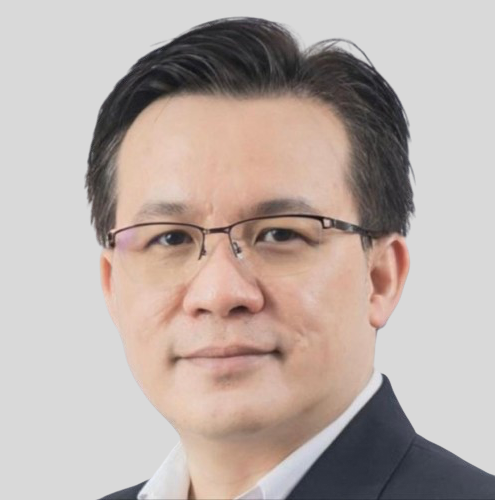
Kam currently serves as Senior Director at TSMC Advanced Packaging Technology and Service, which he joined in 2022. He specifically manages the TSMC Testing RD, Testing operations and backend turnkey operations. He has extensive experience in semiconductor industry, having worked 27 years at Intel, in various roles in technology development, product development and high volume manufacturing. He previously held the role of Vice President of Intel product development and engineering.
Company Profile
TSMC pioneered the pure-play foundry business model when it was founded in 1987, and has been the world’s leading dedicated semiconductor foundry ever since. The Company supports a thriving ecosystem of global customers and partners with the industry’s leading process technologies and portfolio of design enablement solutions to unleash innovation for the global semiconductor industry. With global operations spanning Asia, Europe, and North America, TSMC serves as a committed corporate citizen around the world.
TSMC deployed 288 distinct process technologies, and manufactured 11,878 products for 522 customers in 2024 by providing the broadest range of advanced, specialty and advanced packaging technology services. The Company is headquartered in Hsinchu, Taiwan. For more information please visit https://www.tsmc.com.

14:40 – 15:00
Heterogeneous Integration for Photonic Light Engines
Heterogeneous integration is essential for the manufacturing of higher speed, lower power and highly compact optical components. In this talk we discuss heterogeneous optical integration, where separately manufactured electronic components are assembled on to an active silicon photonics interposer. This process allows for the integration of components independently designed and optimized from several different technology and foundry platforms, including semiconductor lasers onto a common active, optical interposer.

Radha Nagarajan, Ph.D.
Marvell Technology
Dr. Radha Nagarajan is Senior Vice President and Chief Technology Officer of Marvell’s Optical Engineering Group. In this role, he manages the development of the company’s optical platform technology and products. Radha joined Marvell from Inphi, where he served as the Senior Vice President and Chief Technology Officer of Platforms.
In 2025, Radha was elected to the National Academy of Engineering (NAE, US) for his contributions to the advances in high-speed lasers and photonic integration technologies. He has been awarded more than 250 US patents and is a Fellow of the IEEE, OSA and IET (UK). He has also been awarded the IEEE/LEOS Aron Kressel Award, the IPRM (Indium Phosphide and Related Materials) Award and the OPTICA David Richardson Medal, in recognition of breakthrough work in the development and manufacturing of large scale photonic integrated circuits. Radha was named to Electro Optics’ The Photonics100 which honors the industry’s most innovative people. Radha holds a B.Eng. from the National University of Singapore, M.Eng. from the University of Tokyo, and Ph.D. from the University of California, Santa Barbara, all in Electrical Engineering.
Company Profile
We believe that infrastructure powers progress. That execution is as essential as innovation. That better collaboration builds better technology. At Marvell, We go all in with you.
Focused and determined, we unite behind your goals as our own. We leverage our unrivaled portfolio of infrastructure technology to identify the best solution for your unique needs. And we sit shoulder-to-shoulder with your teams to build it. Agile in our thinking, and our partnerships, we look for unexpected connections that deliver a competitive edge and reveal new opportunities. At Marvell, we’re driven by the belief that how we do things matters just as much as what we do. Because, with a foundation built on partnership, anything is possible.


Mark Wade, Ph.D.
Ayar Labs
Mark is Chief Executive Officer and Co-Founder of Ayar Labs. His prior roles at Ayar Labs include Chief Technology Officer and Senior Vice President of Engineering. He is recognized as a pioneer in photonics technologies and, prior to founding the company, led the team that designed the optics in the world’s first processor to communicate using light. He and his co-founders invented breakthrough technology at MIT and UC Berkeley from 2010-2015 which led to the formation of Ayar Labs. He holds a PhD from University of Colorado.
Company Profile
Ayar Labs is disrupting the traditional performance, cost, and efficiency curves of the semiconductor and computing industries by driving a 1000x improvement in interconnect bandwidth density at 10x lower power. Ayar Labs’ patented approach uses industry standard cost-effective silicon processing techniques to develop high speed, high density, low power optical based interconnect “chiplets” and lasers to replace traditional electrical based I/O. The company was founded in 2015 and is funded by a number of domestic and international venture capital firms as well as strategic investors. For more information, visit www.ayarlabs.com.
Address: 695 River Oaks Parkway, San Jose, CA 95134
Phone: 650-963-7200
Email: info@ayarlabs.com

15:25 – 16:25
Networking and Coffee Break Business Meeting Slot 3&4
16:30 – 16:40
Enabling Metrology, Inspection and Lithography Technologies for AI and HPC Packaging
The increasing demand for advanced applications such as artificial intelligence (AI) and high-performance computing (HPC) has driven the greater adoption of the heterogeneous integration of chiplets into advanced packaging technologies. To optimize power, performance, area, and cost for specific applications, integration is pursued at both wafer and panel levels. In this presentation we will discuss key integration technology trends and examine how Onto Innovation’s comprehensive product portfolio addresses these high-value challenges.

Monita Pau, Ph.D.
Onto Innovation
Monita Pau is currently Strategic Marketing Director for Advanced Packaging at Onto Innovation. She works with business leaders and executives to drive strategic planning and leads the development of collaborative initiatives to drive growth and innovation. With over 15 years of experience, her expertise spans across frontend and backend of line process control solutions as well as specialty materials for advanced packaging and assembly. Prior to joining Onto, she held various positions in applications engineering, marketing and strategic business development at DuPont and KLA. Monita holds a Ph.D. degree in Chemistry from Stanford University.
Company Profile
Onto Innovation is a leader in process control, combining global scale with an expanded portfolio of leading-edge technologies that include: Un-patterned wafer quality; 3D metrology spanning chip features from nanometer scale transistors to large die interconnects; macro defect inspection of wafers and packages; elemental layer composition; overlay metrology; factory analytics; and lithography for advanced semiconductor packaging. Our breadth of offerings across the entire semiconductor value chain helps our customers solve their most difficult yield, device performance, quality, and reliability issues. Onto Innovation strives to optimize customers’ critical path of progress by making them smarter, faster and more efficient. Headquartered in Wilmington, Massachusetts, Onto Innovation supports customers with a worldwide sales and service organization.
General Telephone: +1 978 253 6200
General email: info@ontoinnovation.com
Website: www.ontoinnovation.com

16:40 – 16:50
Wet Process and TBDB for Heterogeneous Integration
Wet process and TBDB (Temporary Bonding and Debonding) are important and critical for heterogeneous integration and advanced packaging.

Eric Lee
Scientech
Eric Lee is the CEO of Scientech Corp. and Chairman of Yayatech. He joined Scientech in 2004, following nearly a decade at UMC, where he held positions in both Taiwan and Singapore from 1995 to 2004.
In addition to his leadership roles at Scientech and Yayatech, Eric serves as President of the International Semiconductor Executive Summit (ISES) Taiwan. He is also a part-time professor in the Advanced Packaging Master’s Program at National Taiwan University of Science and Technology.
Eric contributes actively to the industry through his roles as a member of the SEMI Taiwan Advanced Packaging Committee and as a director of the Taiwan Electronic Equipment Industry Association.
Company Profile
Scientech Corporation was established in Taipei, Taiwan in 1979.
What we do: Industries we serve: Semiconductor (front-end, back-end and GaAs), Flat Panel Display, LED, Data Storage, Scientific Instruments and high-tech related industries.
Being a leading semiconductor equipment and wafer reclaim supplier in Taiwan, Scientech Corporation has launched the development of wet process equipment in 2003. Scientech has successively supported customers in LED, Mini/Micro LED, compound semi and power components such as IGBT, SiC and GaN industries, as well as advanced packaging process such as Bumping, Fan-out, Chip-On-Wafer and so on. Our wet process equipment has been successfully verified in the latest Chiplet’s 2.5D/3D packaging process technology and smoothly introduced into mass production.

16:50 – 17:00
Co-Packaged Optics and Solutions for High Volume manufacturing
The rapid development of AI, IoT, 5G and high-performance computing applications has led to exponential growth in data traffic within data centers. Nearly three-quarters of this data traffic remains within the confines of data centers. Traditional pluggable optics cannot keep up with this surge. This is where Co-Packaged Optics (CPO) technology comes into play.
CPO represents a disruptive approach to increasing bandwidth density and energy efficiency. It achieves this by significantly reducing electrical interconnect lengths through advanced packaging and simultaneously optimizing electronics and photonics. Particularly on the silicon platform, CPO holds promise for future data centers.
International companies such as Intel, Broadcom, and IBM have heavily invested in CPO technology. This interdisciplinary research field encompasses photonic devices, integrated circuit designs, packaging, modeling of photonic components, electronic-photonics co-simulation, applications, and standardization.
The challenges in CPO production are diverse. These include integrating electronics and photonics, developing reliable packaging technologies, and standardization efforts. Nevertheless, CPO offers tremendous potential for the future of data center connectivity.
ASMPT as a key equipment supplier for CPO applications offers the solutions for high volume manufacturing of Co-Packaged Optics devices.

Dr. Johann Weinhändler
ASMPT Semiconductor Solutions
Holds an Electrical Engineering Degree from the DAG Technikum in Würzburg/Germany , an MBA from the Open University Business School in Milton Keynes/UK and am Ph.D in Economics from the Trinity Colleges in Dublin. He has over 30 years global Sales and Marketing experience in the semiconductor equipment industry. During his career he was working with Lam Research, Datacon, Oerlikon Systems and ASMPT AMICRA.
Company Profile
ASMPT Limited, founded in 1975, is headquartered in Singapore and is listed in Hong Kong Stock Exchange since 1989.
ASMPT is the only company in the world that offers high-quality equipment for all major steps in the electronics manufacturing process – from carrier for chip interconnection to chip assembly and packaging to SMT. No other supplier offers a comparable range and depth of process expertise.
Semiconductor Solutions Segment Business of ASMPT offers a diverse product range from bonding to molding and trim & form to the integration of these activities into complete in-line systems for the microelectronics, semiconductor, camera modules, advanced packaging, photonics, and optoelectronics industries.
The group has successfully established itself as the leading player in the back-end assembly and packaging market with its innovative solutions and constant focus on customer value creation.

17:00 – 17:10
State-of-the art solutions for AI Chip manufacturing
Over the past nine months, the AI chip boom has accelerated considerably. High-bandwidth memory (HBM) chips, which are an essential part of AI chips, are undergoing rapid technological advancements. While temporary bonding will still be needed for wafer thinning of HBM3 chips and following generations, production of HBM chips is supposed to shift from thermal compression (TC) bonding to hybrid bonding solutions. TC may still be the preferred option for HBM4, as hybrid bonding is significantly more expensive. However, with HBM5 at the latest, the switch to hybrid bonding is expected to take place due to higher I/O densities. SUSS MicroTec has developed a D2W hybrid bonding solution together with flip-chip bonder specialist SET and also offers W2W hybrid bonding solutions, thus providing the technologies required for the next generations of HBM and AI chips.

Robert Wanninger
SUSS
Robert Wanninger is Senior Vice President of the Advanced Backend Solutions (ABS) business unit at SUSS. With leading equipment and process solutions for Imaging, Coating and Bonding applications, SUSS ABS business unit is well positioned to serve the semiconductor industry. Robert brings ~25 years of experience in semiconductor industry. Prior to joining SUSS in 2021, he has worked over 20 years at Infineon in various management positions and spend two years in Korea as COO of LS Power Semitech. He holds a PhD in Chemistry from the University of Regensburg, Germany.
Company Profile
SUSS is a leading supplier of equipment and process solutions for microstructuring in the semiconductor industry and related markets. In close cooperation with research institutes and industry partners SUSS contributes to the advancement of next-generation technologies such as 3D Integration and nanoimprint lithography as well as key processes for MEMS and LED manufacturing. With a global infrastructure for applications and service SUSS supports more than 8,000 installed systems worldwide. SUSS is headquartered in Garching near Munich, Germany. For more information, please visit suss.com.
Company Products & Services
The SUSS portfolio covers a comprehensive range of products and solutions for backend lithography, wafer bonding and photomask processing, complemented by micro-optical components. After sales, the company supports the entire life cycle of the tools: its range of services begins with the installation and startup of the systems including user training. Once systems are integrated in the customer’s environment, SUSS provides consistent support. Since long life cycles are very common for the company’s equipment, preventive maintenance programs are available, as well as reliable spare parts systems, warranty extensions and system upgrades. SUSS maintains service locations and local support teams in all areas of the globe to provide quick help.

17:10 – 17:20
The Impact of PulseForge’s Photonic Debonding on Temporary Bonding and Debonding Processes
PulseForge is at the forefront of semiconductor technology innovation. This presentation highlights our flagship photonic debonding (PDB) technology and its transformative impact on Temporary Bonding and Debonding (TB/DB) processes. PDB technology utilizes broadband light (200 nm – 1100 nm) from flashlamps, paired with an engineered light-absorbing layer, to achieve superior results in wafer thinning, Fan-out, and substrate transfer applications.
As TB/DB processes become increasingly prevalent, particularly with high-bandwidth memory chips and other advanced packaging applications, our presentation provides a comprehensive assessment of PDB’s effectiveness with thinned silicon wafers. We also offer a comparative yield analysis of devices as fab-out and post-TBDB processes with photonic debonding. Furthermore, we will emphasize the substantial cost of ownership benefits that PDB offers, demonstrating clear advantages of PDB over traditional debonding processes and making it a compelling choice for semiconductor manufacturers looking to enhance performance and reduce costs.
The PDB features a uniform, large-area illumination (75 mm x 150 mm), ensuring enhanced yield, high throughput, and cost-effectiveness for both wafer-level and panel-level packaging.

Vikram Turkani
PulseForge
Vikram Turkani, serves as the Director of Technology Partnerships and Strategic Business Development at PulseForge Inc., a prominent technology company specializing in advanced packaging solutions based in Austin, Texas. In this pivotal role, Vikram is instrumental in steering the development and implementation of cutting-edge technologies at PulseForge. Through close collaboration with global technology partners, he ensures the successful transition of these state-of-the-art solutions into practical applications within the market.
Beyond driving the development of innovative technologies, Vikram actively engages with PulseForge’s customers, facilitating the seamless adoption of these innovations on a large scale. In addition to his professional pursuits, Vikram enjoys hiking Texas hill country and exploring the vibrant Austin food scene.
Company Profile
PulseForge, Inc. develops and manufactures state-of-the-art flashlamp-based tools that deliver energy in a precise and targeted manner to enable innovation in industrial manufacturing. Our expertise and tools empower our customers to explore novel materials and manufacturing methodologies, driving dynamic and efficient production at an industrial scale.

17:20 – 17:30
Innovative laser assisted bonding processes for next generation advanced packaging
Conventional assembly techniques like thermo-compression bonding, oven reflow, or thermossonic wire bonding introduce high thermal and mechanical stress into the contacts and the entire semiconductor package, leading to warpage, cracks, or delamination effects. Moreover, the increasing significance of the IMC-layer becomes crucial when considering further miniaturization roadmaps of solder-based contacts << 16μm using these conventional bonding processes. To address this, “PacTech” has been developing laser-assisted processes since 1995, which enable high dynamic local and selective heating and are therefore ideal for next-generation advanced packaging. Laser-assisted reflow (LAR) of C4 bump arrays and SMD-populated substrates, laser-assisted chip bonding (LAB) and debonding processes (LAdB) as well as laser-soldered wire bonding (SB²-WB) for high-power devices, will be introduced and explained as alternative bonding solutions.

Matthias Fettke
PacTech
Company Profile
PacTech-Packaging Technologies GmbH, established 1995 and a group company of NAGASE & CO., LTD., manufactures equipment for the microelectronic & advanced packaging industry and offers wafer level bumping & packaging contract manufacturing out of Nauen, Germany (HQ), and through the 100% subsidiaries PacTech USA Inc., Silicon Valley, USA and PacTech ASIA Sdn., Bhd., Penang, Malaysia.
The equipment product line consists of solder jetting equipment (SB2-Jet), wafer-level solder ball transfer systems (Ultra-SB2), wafer-level solder rework equipment (Ultra-SB2 300 WLR), laser assisted (LAB, LCB, LAR) flip-chip bonders (Laplace) and automatic wet chemical lines for high volume electroless NiAu & NiPdAu bumping (PacLine 300 A50).
Those unique and highly innovative manufacturing systems are providing solutions for today’s tasks and challenges in advanced packaging applications.
The wafer level packaging & bumping subcontractor services consist of electroless Ni/Au, Ni/Pd and Ni/Pd/Au Under Bump Metallization (UBM) for either wafer level solder bumping for Flip Chip or WLCSP or for wire bonding. Additionally, PacTech offers AOI, X-Ray, SEM, BCB Repassivation, wafer-level redistribution, wafer backside metallization, wafer thinning, laser backside marking, wafer dicing, chip singulation, tape & reel services.

17:30 – 17:50
Disruptions in Semiconductor Supply Chain
a. We have been working with 3000+ global executives to reveal the level of disruption across various sectors and the driving force behind
b. The recent result shows semiconductor is experiencing more distruption than others
c. The driving forces behind are a few technology advancement, supply chain rebalancing driven geopolitical tension and customer demands
d. We have helped many of them take concrete actions to smooth the disruption from various topics
f. The key trends in supply chain rebalancing and our take-aways for TW semiconductor sectors
Michael Mo
AlixPartners
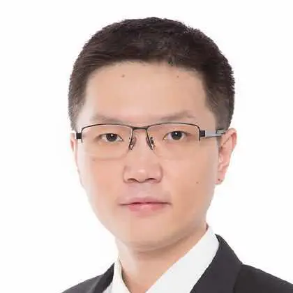
Michael is a proven business leader specializing in helping organizations drive business improvement through operation transformation and create sustainable growth. He brings more than 20 years of experience in strategy development and value creation and has served clients across a full spectrum of businesses, including high-tech and semiconductor sectors. Prior to joining AlixPartners, Michael was a Partner at EY-Parthenon and headed its strategy-to-transformation operation service line in APAC, He also held leadership roles in McKinsey, Johnson & Johnson and SAP. Michael holds a master’s degree in business administration from the IMD in Switzerland.
Company Profile
AlixPartners is a results-driven global consulting firm that specializes in helping businesses respond quickly and decisively to their most critical challenges—from urgent performance improvement to complex restructuring, from risk mitigation to accelerated transformation. These are the moments when everything is on the line—a sudden shift in the market, an unexpected performance decline, a time-sensitive deal, a fork-in-the-road decision. We stand shoulder to shoulder with our clients until the job is done, and only measure our success in terms of the results we deliver.
Company Products & Services
Clients call us when they need pragmatism and cut-through to solve their most complex challenges arising from a continually disrupted world. Our services cover Artificial Intelligence, Corporate Strategy & Transformation, Data Governance, ESG, Growth, Investigations, Disputes & Advisory Services, Mergers & Acquisitions, Organizational Transformation, Supply-Chain Management & Operations, Technology, Transformative Leadership and Turnaround and Restructuring.

17:50 – 17:55
Closing Address

Kamel Ait Mahiout
Kamel Ait Mahiout is a seasoned professional with over 30 years of experience in the electronics industry. His expertise spans from RF and Microwave engineering to executive roles in prominent companies such as Unity SC and Amkor Technology, where he significantly contributed to the growth and alignment of the businesses with key industry players.
18:15 – 18:30
Dinner Check-in on 3F Ballroom
18:30 – 21:30
Gala Dinner Sponsored by Intel
18:30 – 18:35 Intel Welcome Speech
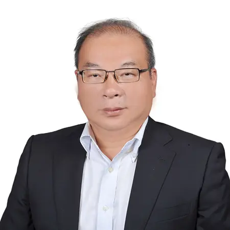
Dr. Yu-Wen Huang
Intel Corporation
Dr. Yu-Wen Huang is an experienced technologist and system supply chain professional with more than 27 years of working in outsourced semiconductors industry. He is currently the Intel Hsinchu site manager, responsible for site operations and engaged in advanced packaging R&D. Prior to his current undertaking, he was instrumental in driving the assessment and adoption of the China Supply Chain ecosystem that supports various IA platforms like tablets, smart phones, and PC products in China. He led the Global Tech Ecosystem (GTE) Operations team that helped grow Client Computing China biz by enabling China Tech Ecosystem (CTE) ODMs to adopt IA PC roadmap platforms and achieve continuous revenue growth. In 2015 Yu-Wen’s was awarded the prestigious Intel Achievement Award (IAA) for being part of the team that drove 40Mu shipment of IA tablets in China. Before taking the China assignment in 2008, he had been managed Taiwan assembly/test outsourcing operations involving top tier foundries and OSATs for 8 years. Dr. Huang received his Ph.D. in Industrial Engineering from State University of New York, Binghamton. He then joined Institute of Microelectronics (IME), Singapore as Member of Technical Staff from 1997 to 2000, with primary focus on MCM-D module development, UBM characterization, and flip chip bumping process development. He also led FCBGA development programs in the IME initiated consortium.
Company Profile
Intel (Nasdaq: INTC) is an industry leader, creating world-changing technology that enables global progress and enriches lives. Inspired by Moore’s Law, we continuously work to advance the design and manufacturing of semiconductors to help address our customers’ greatest challenges. By embedding intelligence in the cloud, network, edge and every kind of computing device, we unleash the potential of data to transform business and society for the better.
To learn more about Intel’s innovations, go to newsroom.intel.com and intel.com.

End of content
End of content